
Design Tradeoffs
12. Design Tradeoffs
The circumspect engineer, given a problem to solve, inevitably faces a wide range of plausible alternative design choices. Typically, alternative paths to solving a problem differ in various cost and performance parameters, including- Hardware cost measures: circuit size, transistor count, etc.
- Performance measures: Latency, throughput, clock speed.
- Energy cost measures: average/maximum power dissipation, power supply and cooling requirements .
- Engineering cost measures: design ease, simplicity, ease of maintenance/modification/extension.
Optimizing Power
12.1. Optimizing Power
We noted in Section 6.5 that the primary cause of power dissipation within CMOS logic circuitry is ohmic losses in the flow of current into and out of signal nodes during logic transitions. As observed in that section, the power dissipated is proportional to the frequency of transitions, which, in typical circuitry, is proportional to the clock frequency. In many situations we can improve the average (or maximum) energy dissipation by choosing a design that minimizes the number of logic transitions per second. A simple way to achieve that goal is by lowering the clock frequency, usually at a proportional loss of processing performance; indeed, some modern computers have low-power operating modes which simply slow the clock to a fraction of its maximal rate.Eliminating Unnecessary Transitions
12.1.1. Eliminating Unnecessary Transitions
Can we lower the rate of transitions without commensurate performance degradation? Often the answer is yes. Consider, for example, the design of an Arithmetic Logic Unit (ALU), a high-level combinational building block you will be familiar with from the laboratory. An ALU is a computational Swiss army knife, performing any of a repertoire of operations on its input data based on a multi-bit function code (ALUFN) passed as a control input.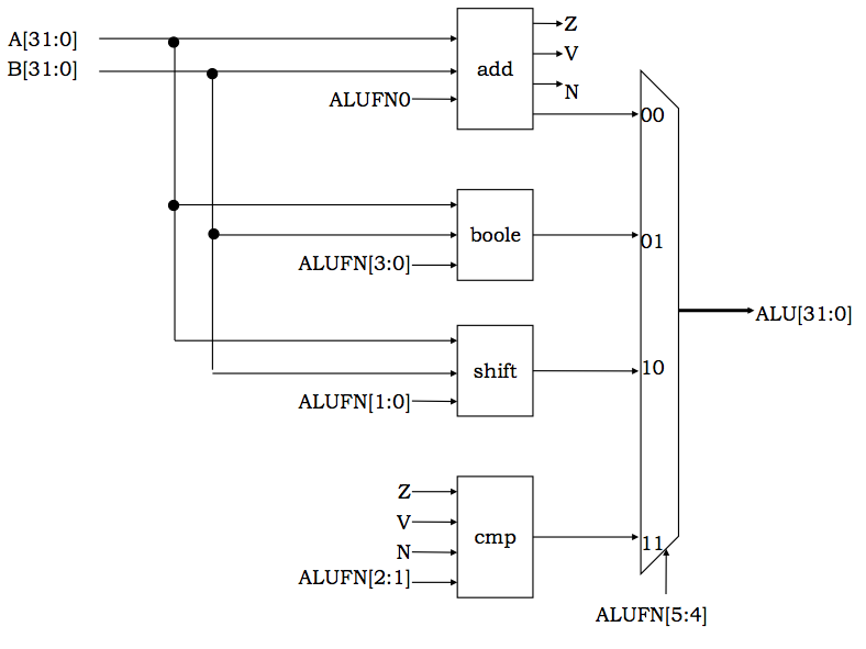
Typical ALU Block Diagram
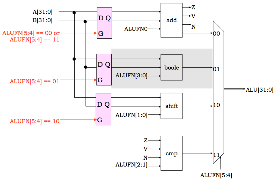
Power-saving ALU Design
Optimizing Latency
12.2. Optimizing Latency
We can often use the mathematical properties of operations performed by circuit elements to rearrange their interconnection in a way that performs equivalent operations at lower latency. A common class of such rearrangements is the substitution of a tree for a linear chain of components that perform an associative binary operation, mentioned in Section 7.7.2.Parallel Prefix
12.2.1. Parallel Prefix
We can generalize this approach to other binary operations. Suppose $\circledast$ is an associative binary operator, meaning that $a \circledast (b \circledast c) = (a \circledast b) \circledast c$. We can generalize this operator to $k$ operands $x_0, x_1, ... x_{n-1}$ by iteratively applying the binary $\circledast$ operator to successive prefixes of the operand sequence, computing each intermediate $x_j \circledast ... \circledast x_0$ by the recurrence $x_j \circledast (x_{j-1} \circledast ... \circledast x_0)$, generating values for each successive prefix of the argument sequence. This imposes a strict ordering on the component applications of the binary $\circledast$ operator; it requires that the result of applying $\circledast$ to the first $j-1$ arguments be completed before it is applied to $x_j$. In a sequential circuit implementation, the $k$-operand function would take $\theta(k)$ execution time, sufficient for a sequence of $k$ binary operations. A corresponding combinational circuit would have an input-output path going through all $k-1$ components, again implying a $\theta(k)$ latency. The associativity of $\circledast$, however, affords some flexibility in the order of the component computations. We can use the fact that $$x_0 \circledast (x_1 \circledast (x_2 \circledast x_3)) = (x_0 \circledast x_1) \circledast (x_2 \circledast x_3)$$ to process pairs of arguments in parallel, reducing the number of operands to be combined by a factor of two in the time taken by one binary operation. Repeated application of this step -- halving the number of operands in a single constant-time step -- reduces the asymptotic latency from $\theta(k)$ to $\theta(log(k))$, a dramatic improvement. In a combinational implementation, it results in a tree structure like that of Section 7.7.2. The key to this (and other) latency reduction techniques is to identify a critical sequence of steps that constrains the total execution time, and break that sequence into smaller subsequences that can be performed concurrently.Carry-Select Adders
12.2.2. Carry-Select Adders
Returning to the problem of binary addition, we have observed that the critical sequence through the ripple-carry adder of Section 11.2 is the combinational path that propagates carry information through each full adder from low-order to high-order bit positions. We might (and generally do) aspire to minimize the delay along this path by careful design of our full adder component to produce the output carry as fast as possible; however, this optimization gives at best a constant factor improvement to our $\theta(N)$-bit latency. More dramatic improvements require that the carry chain somehow be broken into pieces that can be dealt with in parallel. Suppose we need a 32-bit adder, but are unhappy with the latency of a 32-bit ripple-carry adder. We might observe that the latency of a 16-bit adder is roughly half that number, owing to its shorter carry chain; thus we could double the speed of our 32-bit adder by breaking it into two 16-bit adders dealing in parallel with the low- and high-order halves of our addends. The problem is that the carry input to the high-order 16-bit adder is unknown until the low-order adder has completed its operation.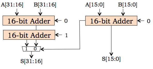
Carry-select Adder
Carry-Lookahead Adders
12.2.3. Carry-Lookahead Adders
It is tempting to try rearranging the full adders of a ripple-carry adder in a tree, in order to get the $\theta(log n)$ latency available to $n$-bit associative logical operations like AND and XOR. Of course, the functions performed by the full adders cannot be arbitrarily regrouped, since the full adder at each bit position takes as input a carry from the next lower-order position, and supplies a carry to the adjacent higher-order full adder. This would seem to rule out performing the function of the higher-order FAs simultaneously with that of lower-order ones. Clever reformulation of the building blocks used for our adders, however, can mitigate this constraint. The key to our new approach is to eliminate carry out signals, which necessarily depend on carry inputs (leading to the $\theta(n)$ carry chain), replacing them with alternative information that can be used to deduce higher-order carry inputs. We'd like the new outputs to have two key properties:- They can be generated from the $A_i$ and $B_i$ inputs available at each bit position from the start of the operation, not depending on outputs computed from other bit positions;
- Information from two adjacent sequences of bit positions can be aggregated to characterize the carry behavior of their concatenation.
- Generate: Given these $A$ and $B$ values, $C_{out} = 1$ always.
- Kill: Given these $A$ and $B$ values, $C_{out} = 0$ always.
- Propagate: Given these $A$ and $B$ values, $C_{out} = C_{in}$, where $C_{in}$ is the carry input to the low-order bit of the adder.
- G (generate): $1$ if the carry is $1$;
- P (propagate): $1$ if the carry is $C_{in}$.
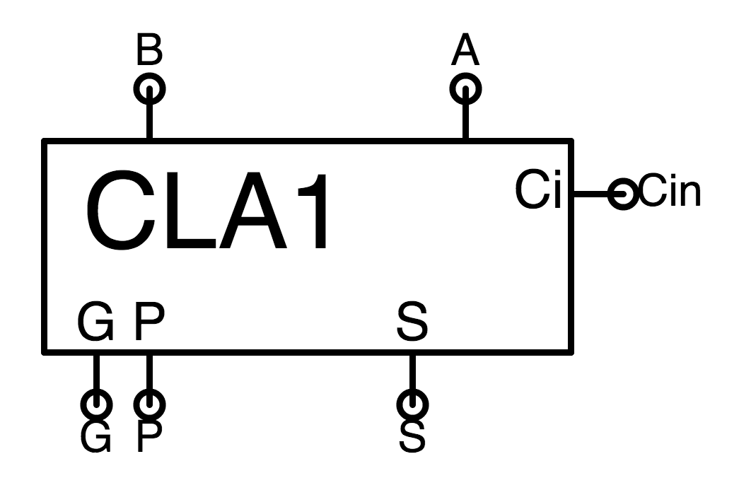
1-bit CLA
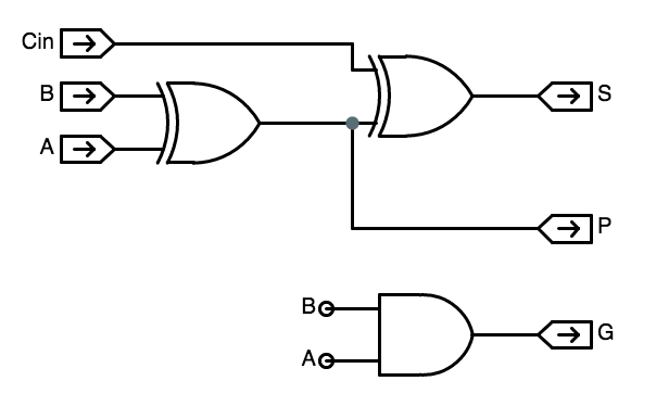
1-bit CLA logic
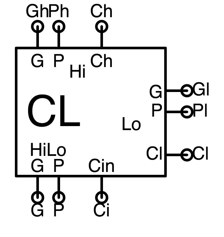
2-bit CLA circuit
2-bit CLA
-
It combines $G_h, P_h$ and $G_l, P_l$ signals from the high- and low-order component adders to generate appropriate $P$ and $G$ signals for their combination. The combined $P = P_h \cdot P_l$ and $G = G_h + P_h \cdot G_l$ are generated by the logic shown to the right.
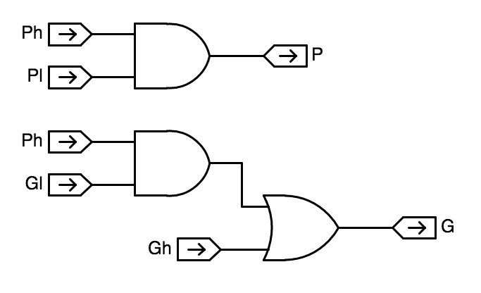
CL GP logic - It generates carry input signals $C_h$ and $C_l$ for the component
adders.
The carry input to the low-order component is just the carry input to
the combined adder; it is the $C_{in}$ input to the CL component. The carry input to the high-order component is computed using the $P$ and $G$ inputs computed in the step above, using the pair of gates shown to the right.
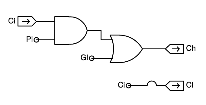
CL carry logic
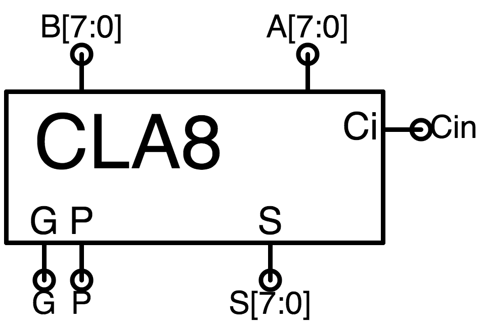
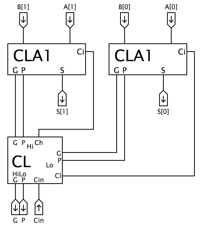
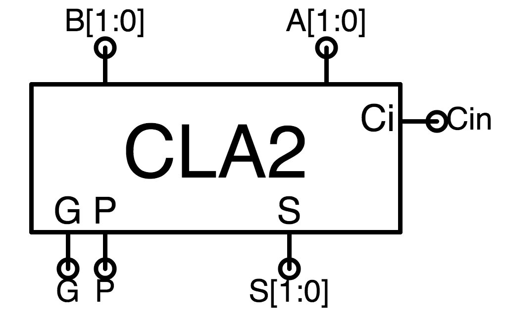
8-bit CLA
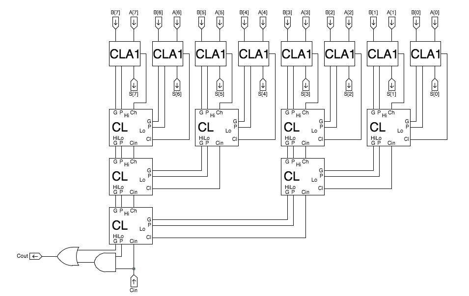
8-bit CLA, expanded
Optimizing Throughput
12.3. Optimizing Throughput
The most obvious way to improve the throughput of a device that computes $P(X)$ from $X$ is brute-force replication: if the throughput of one device is $T_P$ computations/second, then $N$ copies of the device working in parallel can perform $N \cdot T_P$ computations/second. In Section 11.5 we introduced the notion of pipelining, which often affords cheaper throughput improvements by adding registers rather than replicating the logic that performs the actual complication. These two techniques can often be combined to optimize throughput at modest cost. However, computation-specific engineering choices can dramatically impact their effectiveness and the performance of the resulting design.N-bit Binary Multiplier
12.3.1. N-bit Binary Multiplier
Consider, for example, the multiplication of two $N$-bit unsigned binary numbers $A_{N-1:0}$ and $B_{N-1:0}$ to produce a $2 \cdot N$-bit unsigned binary product $P_{2N-1:0}$. We may view this operation as the sum of $N$ partial products, each of the form $B_i \cdot A_{N-1:0} \cdot 2^i$ for $0 \leq i \lt N$. Observe that each partial product can be formed by $N$ AND gates, multiplying the bits of $A$ by a selected $B_i$. It remains to sum the $N$ partial products, which we can do using an array of full adders -- much like our $N$-bit by $M$-word adder of Section 11.4. To streamline our design, we devise a multipler "slice" component containing $N$ full adders with an AND gate on one sum input, and replicate this slice component for each of the $N$ partial products. Our resulting design has the following structure: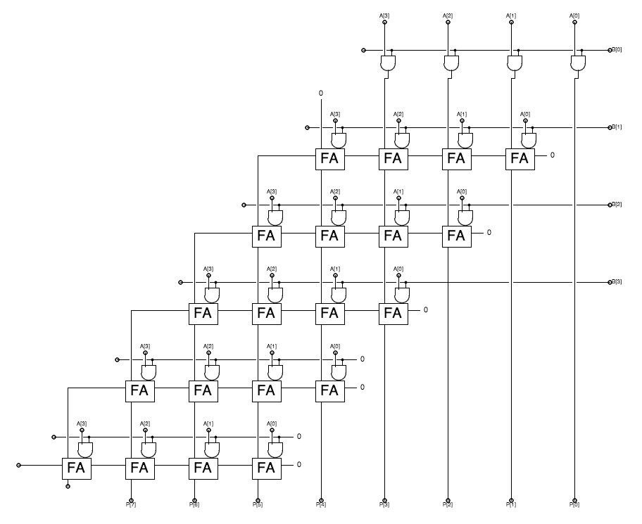
4-bit Multiplier
Pipelined Multiplier
12.3.1.1. Pipelined Multiplier
If we have a large number of independent multiplications to perform, it seems logical to pipeline our $n$-bit combinational multiplier to improve its $\theta(1/N)$ throughput. Quick inspection of the $4$-bit multiplier diagram above suggests an obvious partitioning of the combinational circuit into pipeline stages: each horizontal slice, that forms a 4-bit partial product and adds it to the sum coming from slices above, might constitute a pipeline stage. Indeed, we could pipeline our multiplier by drawing stage boundaries between horizontal slices, and inserting registers wherever a data path intersects a stage boundary. Unfortunately, such a pipelining approach would not result in improved performance. Since each multiplier slice effectively contains an $N$-bit ripple-carry adder, it requires $\theta(N)$ time for the carry to propagate from right to left through all $\theta(N)$ bits. The maximal clock period is thus $\theta(N)$, and the throughput of our naively pipelined multiplier remains at $\theta(1/N)$. Since there are $\theta(N)$ stages, however, the latency has now been degraded from $\theta(N)$ to $\theta(N^2)$. To materially improve performance, we must find a way to break long ($\theta(N)$) paths within each pipeline stage. The problem with our naive pipeline is that our horizontal pipeline boundaries failed to break up the horizontal carry chains within each slice. We might address this problem by making either the pipeline stage boundaries or the carry chains less horizontal, so that they intersect. The latter approach is deceptively simple: rather than routing the carry output from each full adder to the full adder on its immediate left, we route the carry to the corresponding full adder in the slice below.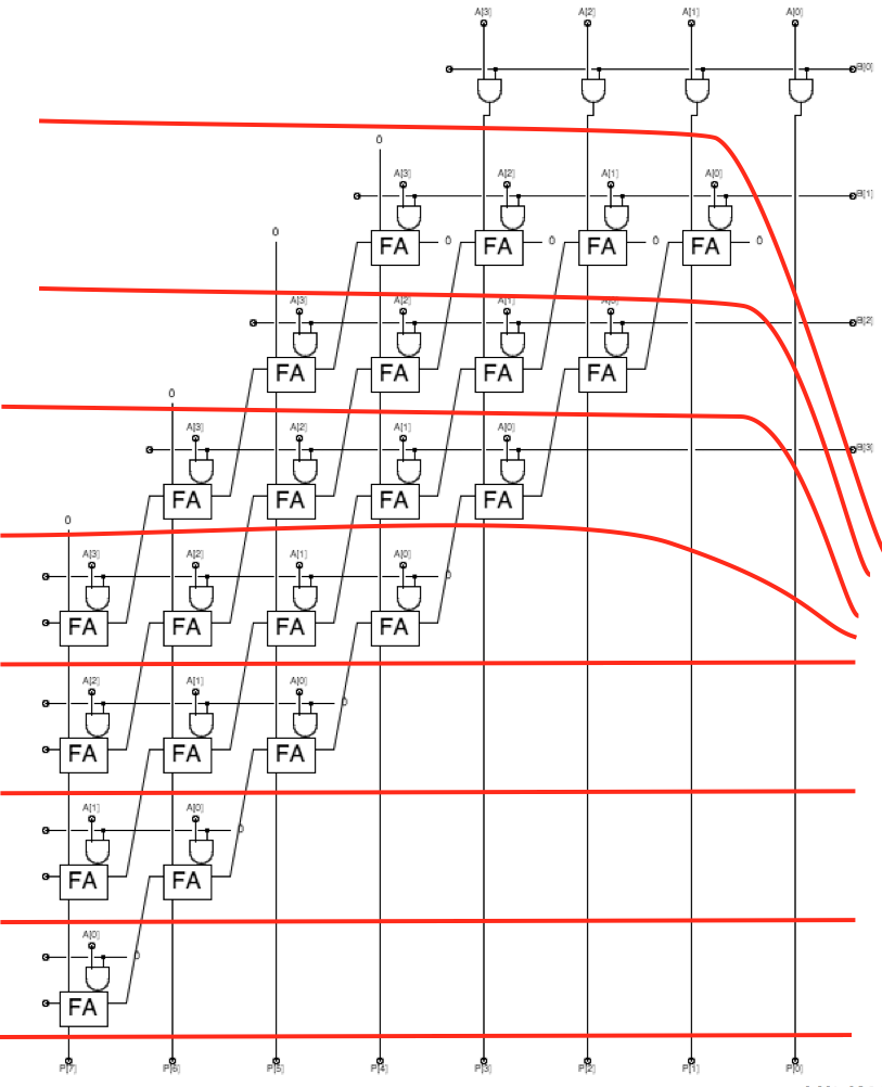
4-bit Multiplier, pipelined
Sequential Multiplier
12.3.1.2. Sequential Multiplier
The $N$-bit pipelined multipler just sketched can be built using $\theta(N)$ idential "slices", each a module containing $N$ each AND gates and full adders; we note that the topmost slice in our diagram omits the full adders, optimizing for the case when the sum coming from the slice above is zero. In pursuit of high throughput, at any instant each of the identical slices of our pipelined problem will be working on a different multiplication operation; hence any single multiplication is only using one of the slices at a time.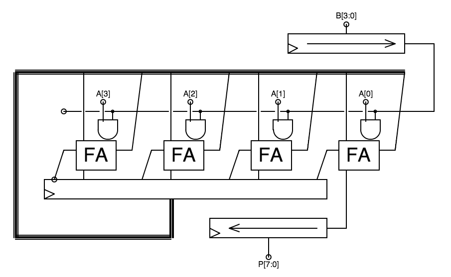
4-bit Sequential Multiplier
Multiplier Recap
12.3.1.3. Multiplier Recap
The design of state-of-the-art multipliers involves a number of engineering techniques beyond our current scope; the three design examples here are chosen to illustrate tradeoffs typical of basic design decisions.
| Design | Cost | Latency | Throughput |
|---|---|---|---|
| Combinational | $\theta(N^2)$ | $\theta(N)$ | $\theta(1/N)$ |
| Pipelined | $\theta(N^2)$ | $\theta(N)$ | $\theta(1)$ |
| Sequential | $\theta(N)$ | $\theta(N)$ | $\theta(1/N)$ |
Chapter Summary
12.4. Chapter Summary
This chapter explores, via simple examples, the sorts of engineering tradeoffs confronted during the design process. Among the salient observations of this chapter:- Power dissipation, typically proportional to the frequency of logic transitions, can be optimized by minimizing the number of transitions made during a computation.
- Minimization of combinational latency involves shortening the propagation delay along the longest input-output path. For a broad class of functions, this can be done using a tree structure, reducing the latency of an $N$-input function to $\theta(log N)$.
- Pipelining improves throughput so long as stage boundaries break long combinational paths.
- Sequential designs can exploit recurring structure replicating their function in time rather than in hardware, saving hardware cost.