Sequential Logic
8. Sequential Logic
An important characteristic of combinational circuits is
their inherent
finiteness: every combinational
circuit
- is composed of finitely many gates;
- has finitely many inputs and outputs;
- has finitely many input-output paths;
- performs finitely many basic logical operations
to compute its output;
- takes a finite amount of time -- bounded by its $t_{PD}$
specification -- to perform its computation;
and
- has a finite functional specification (in the form of
a truth table or finite Boolean expression).
While the finiteness of combinational circuits has some
advantages, it limits the set of computations they can
perform. We can design, for example, a combinational device
capable of adding two 32-bit binary numbers and generating
a 32-bit result, a useful building block that will be explored
in subsequent chapters.
Suppose, however, we need to add a column of N 32-bit numbers
for some N greater than two.
We could design a combinational adder having N 32-bit inputs,
a task that becomes tedious for large N; but such a device
would be incapable of adding N+1 numbers when the need arises.
The fixed, finite hardware resources of any combinational device
we build will limit the set of computations it can perform by bounding
the number of inputs accepted and the number of logical operations
performed in the computation.
To deal with a broader set of computations not amenable to
such bounds, such as the addition of N numbers for arbitrary
finite N, we need a way to somehow relax these bounds.
A resourceful accountant faced with this problem would
recognise that adding a column of N numbers can be decomposed
into a
sequence of 2-input additions, each adding a new
input to an accumulating sum.
In effect, the finiteness constraint of his combinational
tool is circumvented by expansion in another dimension:
time.
In this chapter, we explore the liberation of our digital circuits
from the finiteness bounds of combinational logic by technology
and engineering disciplines that allow circuits to perform
sequences of consecutive operations.
The resulting expanded class of digital circuits are historically
called
sequential circuits, meaning that they respond
to time-ordered sequences of input data rather than producing outputs
that reflect only current inputs.
System State
8.1. System State
Our repertoire of combinational devices is clearly missing a
critical function if it is to perform useful sequences of
operations:
memory of some piece of information
that persists from one step of the sequence to the next.
There needs to be an evolving record of
system state,
capable of changing from one step of the sequence to the next
and of affecting the computation at each step; without such
state information, the second and subsequent steps of the
sequence would duplicate the first, without any cumulative
benefit.
The accountant using a 2-input adder to add N numbers must
provide this memory of system state -- the accumulating sum -- by means external to
his combinational adder; if we are to mechanize his approach
in a sequential circuit, we need a device capable of performing
an analogous memory function.
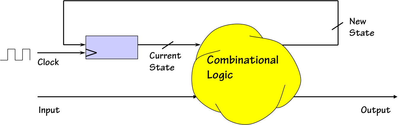
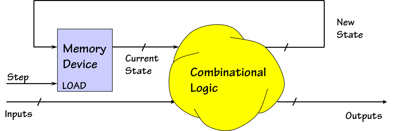 Sequential Circuit
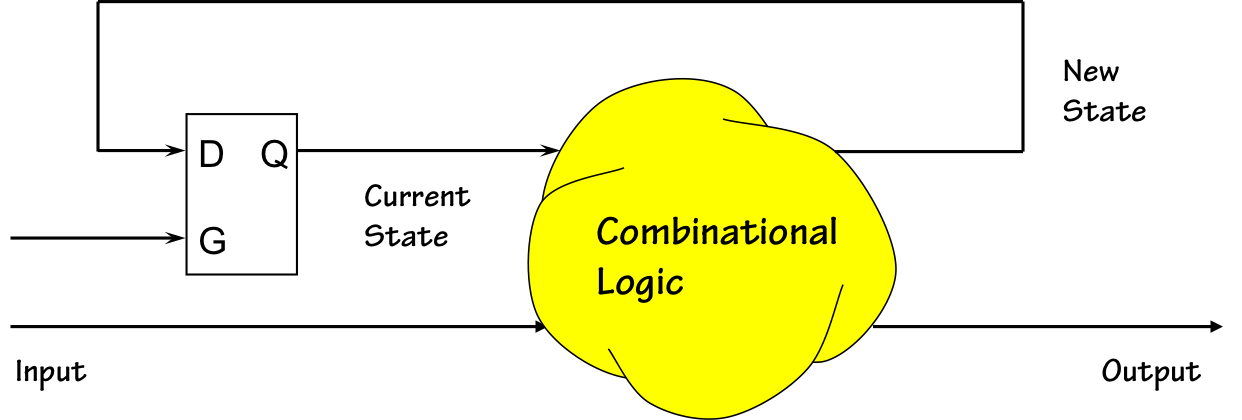
One model of sequential circuits is shown to the right.
It includes a digital
memory device capable of
storing some finite number of bits representing the system's
current state, as well as a block of combinational logic
whose function is to compute both system outputs and a new state
from the current state and system inputs.
In addition to other binary inputs and outputs, the sequential circuit
has a
Step input by which it can be instructed to move from
one step in its sequence of operations to the next. When
Step
is signaled, the memory is loaded with the new state information at its
inputs, discarding the previously stored state. Conceptually, the
system moves from the state encoded in the previously stored bits to a
new state encoded by the bits just loaded into memory.
An important functional distinction between this model and pure
combinational logic is that the outputs produced at each step
of the sequential circuit's computation may reflect the current
system state as well as the current inputs. The current state
will typically reflect some aspect of the system's history, e.g.
the accumulated sum of previously entered addends.
Storage Devices
8.2. Storage Devices
A technology that is missing from our combinational logic toolkit
is the memory device needed to communicate state information between
steps of our sequence.
Many different technologies can be used to effect the storage of
digital information, including electromechanical, chemical, audio,
and optical approaches; the history of digital systems is rich
in interesting and often clever memory designs. Some memory
technologies are
volatile, holding information for
brief periods (so long as power is supplied); others, like
magnetic memories or punched cards provide nonvolatile storage.
We present a brief glimpse of two widespread memory technologies in
Section 8.4: a volatile approach used for computer
main memories using charged capacitors to hold individual bits,
as well as nonvolatile magnetic memory used in disk systems for
files and other longer-term storage needs.
However, the memory technology primarily used for small, short
term information like the state of a sequential circuit is
typically constructed directly from combinational gates, using
carefully-constructed feedback loops to effect a bistable (2-state)
digital device.
The introduction of cycles (and hence feedback) in circuits of
combinational components seems deceptively simple, but requires
tedious attention to engineering detail to design provably reliable
storage devices.
In
Section 8.2.1 we endure this tedium once to build a
single-bit storage device, the
flip flop, and use this
as our basic building block for the storage needs of our sequential
circuits.
Bistable Circuits
8.2.1. Bistable Circuits
In this section, we will explore the "bootstrapped" construction
of memory devices from combinational logic. The key insight
behind this construction is that, by introducing cycles in a
circuit containing combinational logic, it is easy to create
circuits that have multiple stable states in the logic domain.
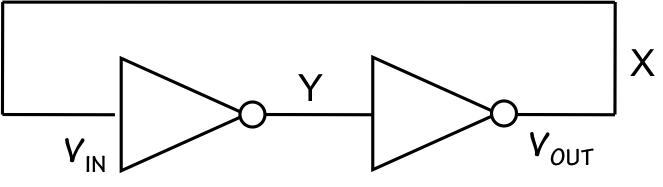 Bistable Circuit
Consider, for example, the simple two-inverter loop shown to the right.
Given our understanding of the behavior of inverters in the logic domain,
It is easy to convince oneself that this circuit exhibits two stable
states -- with the node marked $X$ representing a valid $0$ or $1$,
respectively, and the other node $Y$ representing the opposite value.
In fact, this intuition reflects the only two solutions to constraints
on these logic values imposed by the specifications of the inverters:
namely, that $X = \bar Y$ and $Y = \bar X$.
Which of the two states the circuit is in can be used to store a
single bit of information, suggesting an easy path for the creation
of simple memory devices using combinational logic.
While this approach can be made to work, the simple logic-domain
analysis above seriously understates the engineering complexities
involved.
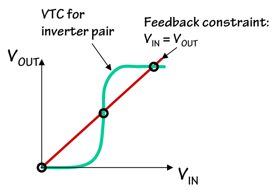
While it is true that the $X=0$ and $X=1$ states are the only solutions
admitted by this circuit in the logic domain, at the circuit level
the analysis is more complex. Consider the two-inverter cascade as a
single device whose voltage transfer characteristic looks like the green
curve shown to the left. This represents one constraint, expressed in
the voltage domain, on its input and output voltages $V_{IN}$ and $V_{OUT}$.
The feedback connection introduces a second constraint $V_{IN}=V_{OUT}$,
shown in red on the $V_{IN}$/$V_{OUT}$ curve. If we solve these two
equations that represent simultaneous constraints on $V_{IN}$ and $V_{OUT}$,
we find solutions wherever the two curves cross.
We do find solutions corresponding to valid $X=0$ and $X=1$ values in the
logic domain; however, the geometry of the intersecting curves is such that
they inevitably cross at a third point between these two solutions.
This third voltage-domain solution represents a problematic
unstable
equilibrium, and is dealt with at length in
Chapter 10.
This third equilibrium typically represents an invalid logic level, and
sequential circuits require a carefully designed engineering discipline
to avoid failures due to propagation of consequent invalid logic levels.
D Latch
8.2.1.1. D Latch
Although we may view the two-inverter loop as a device capable of
storing a bit of information, it is of little use unless we can
exercise some control over the stored bit.
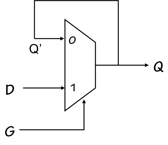
To effect such control, we will use a slightly more complicated
combinational device -- a lenient 2-way multiplexor -- in a similar
feedback loop as shown to the right.
This circuit has a data input $D$ and a control input $G$ (for "gate").
The logic-domain analysis of this circuit is, once again, appealingly
simple: when $G=1$, the logic value on the $D$ input is selected
as the output $Q$ of the device; when $G=0$, the feedback path
from the output $Q$ to the input $Q'$ is selected.
When $G=0$ there are again two stable solutions in the logic
domain: $Q=Q'=0$ and $Q=Q'=1$.
Our intention in this design is to use the $G$ input to switch between two modes
of operation detailed to the left: a $G=0$ mode where the $Q$ output reflects
a stored value, and a $G=1$ mode in which the value on $D$ follows a combinational
path to the $Q$ output.
 D Latch
This device, called a
D Latch, thus behaves as a storage device when
$G=0$ and a "transparent" combinational circuit when $G=1$.
The intent is that a $1 \rightarrow 0$ transition on $G$ switches from transparent
to storage mode, capturing the data currently on $D$ as the newly stored value.
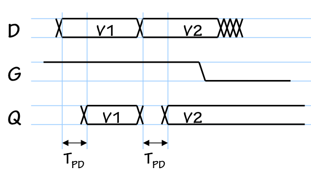
The timing diagram to the left depicts the behavior desired for our latch.
While $G=1$, the output $Q$ reflects the value on the $D$ input after a propagation
delay; changes in $D$ will cause corresponding changes in $Q$. If $G$ becomes
0 while some new value $V2$ is on $D$ (and hence $Q$), the latch will store
$V2$ so long as $G$ remains $0$.
Reliable Latch Operation
8.2.1.2. Reliable Latch Operation
Although capturing the $D$ value on a $1 \rightarrow 0$ transition of $G$
may seem intuitively simple, it confronts subtle obstacles that require
careful attention and for which
lenience plays a critical role.
The use of a non-lenient multiplexor in this circuit would imply
a period of undefined output after
any input change;
once $Q$ is allowed to become invalid, the $Q'$ input is also
invalid, and an invalidity loop may persist even after the $D$
and $G$ inputs are both valid.
Indeed, even a brief contamination of the Q output of the mux
allows invalid levels to circulate around the feedback loop, losing
the stored information; and the mux allows such contamination after
any input change.
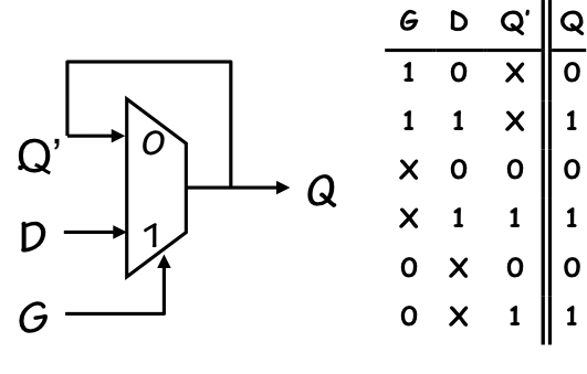
Use of a lenient multiplexor, whose truth table appears to the right,
mitigates this problem by allowing a single input to change under certain
circumstances without contaminating the mux output.
The three circumstances when a mux input may change without contaminating
output validity are:
-
$G=1$, $D=v$ (for $v=0$ or $v=1$)
maintained as valid inputs for at least $t_{PD}$:
$Q=v$ despite changes in the $Q'$ input.
In this case, the $D$ input has been selected as the mux output value; thus
the value on the other data input is immaterial.
-
$D=Q'=v$ (for $v=0$ or $v=1$)
maintained as valid inputs for at least $t_{PD}$:
$Q=v$ despite changes in the $G$ input. In this case, the multiplexor is being
asked to choose between two identical data inputs, so the value on the select
input $G$ is immaterial.
-
$G=0$, $Q'=v$ (for $v=0$ or $v=1$)
maintained as valid inputs for at least $t_{PD}$:
$Q=v$ despite changes in the $D$ input.
In this case, the $Q'$ input has been selected as the mux output value; thus
the value on the other data input is immaterial.
Each of the above lenient-mux guarantees plays a crictical role in the
reliable behavior of our D latch. The first allows valid $G=1$ and $D$ inputs
to force a new value on $Q$, independently of its prior stored value.
The second allows us to change $G$ without contaminating the $Q$ output,
a requirement if we are to "latch" the current $Q$ output.
The third allows us to maintain a stored $Q$ value while $G=0$,
independently of changes on $D$.
There are additional constraints on the timing of our input signals that must be
enforced to ensure reliable latch operation.
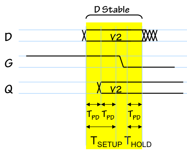 D Latch Timing
To explore the required timing discipline, lets consider the timing of a sequence of
input signals that guarantees the loading of some new value, $V2$, into a latch
made from a lenient multiplexor whose propagation delay is $t_{PD}$.
We assume that the latch is initially in some unknown state.
- The new value, $V2$, is applied to the $D$ input while holding $G=1$.
- After $D$ and $G$ have been valid for $t_{PD}$, the new value $V2$ appears
at the mux output $Q$ (and hence at the input $Q'$.
- After $D$ and $G$ have been valid for $2\cdot t_{PD}$, the $V2$ value
on $Q'$ will have been valid for at least $t_{PD}$.
Thus, the $D$ and $Q'$ inputs are now sufficient to guarantee a valid
$Q=V2$ independently of $G$.
- Continuing to hold $D=V2$, we now change $G$ to $0$.
$Q=Q'$ continues to hold a valid $V2$ during this change.
- After $D=V2$ has been valid for another $t_{PD}$, the $G=0$ and $Q'=Q$
inputs have been valid for a propagation delay and are hence sufficient
to maintain $Q=V2$ independently of $D$. The value $V2$
is now stored in the latch.
Note that, in order to guarantee that the new value $V2$ was reliably loaded
into the latch, we had to maintain a valid $D=V2$ input for a period extending
from at least $2\cdot t_{PD}$
prior to the $1 \rightarrow 0$
transition on $G$ through $t_{PD}$
following that transition.
Intuitively, we must guarantee that transitions on the $D$ and $G$ inputs
to our latch don't come at about the same time: such a race would create
a difficult decision problem of the sort discussed in
Chapter 10.
To avoid such difficulties, we establish a discipline for the
timing of changes on $D$ relative to the active transistion on $G$ for
our latch. In particular, we specify timing parameters $t_{SETUP}$
and $t_{HOLD}$ and require that $D$ must have been stable and valid for
an interval that includes
-
The setup time $t_{SETUP}$ before the transition;
-
The transition time during which the transition occurs; and
-
The hold time $t_{HOLD}$ after the transition;
The setup and hold times for our implementation of the latch are $2 \cdot t_{PD}$
and $t_{PD}$, respectively; although other implementations might have
different values for $t_{SETUP}$ and $t_{HOLD}$, they will typically enforce
the same form of constraint.
Combinational Cycle Problems
8.2.1.3. Combinational Cycle Problems
We might be tempted to try using a latch to store one bit of state for a sequential circuit, as shown
to the right.
Indeed, the latch is capable of holding a "current state" bit so long as its $G=0$;
that state is used to compute a "next state" bit applied to the latch's $D$ input.
However, loading this "next state" bit into the latch is problematic.
Clearly we must raise $G$ to a valid $1$, at least briefly, to load its
new value.
But for how long must $G$ remain $1$?
we note that, while $G=1$, our circuit has a
combinational cycle:
the combinational logic computes a new state bit, which propagates through
the latch to the combinational logic, which then computes a
new new state bit,
etc.
Signals are traveling around this cycle at an uncontrolled rate, and we
have no assurance of when (or even if) we can expect valid logic values.
For this reason, latches are rarely used directly as memory devices in
our digital circuits.
Rather, they are an essential building block for somewhat better behaved
flip flops that we will rely on as our basic storage element.
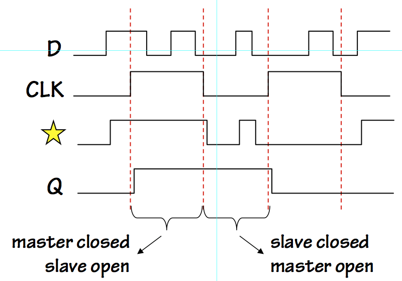
Edge-triggered Flip Flops
8.2.1.4. Edge-triggered Flip Flops
The difficulty in using latches as a memory device in our circuits is that,
in their "transparent" mode, they provide a combinational input-output path.
We can prevent such a path by cascading
two latches and ensuring
that they have opposite values on their $G$ inputs, as shown to the right.
The resulting device has a
clock input $CLK$ used to control the
flow of data from its $D$ input to its $Q$ output. For each value of $CLK$,
exactly one of the two latches -- the
master or the
slave --
is transparent; the other holds a stored value on its output.
 Flip Flop
This device
is called an
edge-triggered or
master-slave flip flop
(or simply
flip flop or
flop)
and is depicted as shown on the left. The $CLK$ input triangle conventionally
represents the clock input to a
clocked device, a class of sequential
devices using edges on their clock inputs to specify timing of critical
events such as loading of new data.
We will build clocked devices using flip flops and combinational logic.
The flip flop shown above has the effect of loading new data from its $D$
input on a positive ($0 \rightarrow 1$) transition on its $CLK$ input.
The diagram to the right shows its behavior given a sequence of changes on its $CLK$
and $D$ inputs. As is typically the case, the $CLK$ input is a periodic square wave.
During the $CLK=1$ phase of its cycle, the master latch is
closed -- outputting
its stored value -- while the slave latch is in an
open or transparent
state, propagating its input value to its output via a combinational path.
During the $CLK=0$ phase, the master is open (propagating any changes on $D$
to the input of the slave) while the slave is closed, maintaining a constant
flip flop output value.
Note that on a positive $CLK$ transition the master latch goes from open to
closed, effectively latching the current data input as its stored value.
This value propagates through to the (transparent) slave and hence to the
flip flop $Q$ output.
The value is latched by the slave on the subsequent negative transition of
$CLK$, but the flipflop output remains unchanged since it matches the
slave input value.
The effect is that the flip flop output value reflects a single stored
bit, which is loaded from $D$ into the flip flop on each positive edge
of $CLK$.
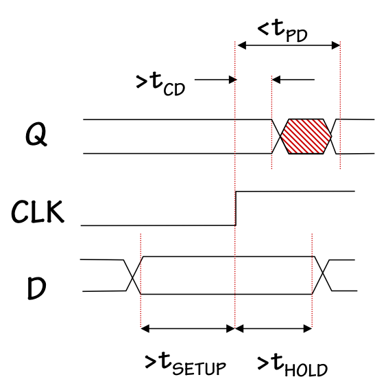 Flip flop timing
We can summarize the timing characteristics of the flipflop as shown in the
diagram to the right.
To load a new value, we again require that the $D$ input
remain stable and valid for an interval that includes prescribed
setup and hold times surrounding the active $CLK$ edge.
These values are chosen to ensure that the setup and hold times of
the component latches are met.
We also characterize the timing of the $Q$ output of the flip flop
by familiar
propagation and
contamination delays.
In contrast to the $t_{PD}$ and $t_{CD}$ of combinational devices,
however, for clocked devices we measure these intervals relative to
the active clock edge.
Thus, as depicted in the above diagram, the $Q$ output will maintain
its previous value for at least $t_{CD}$ following the start of an
active $CLK$ edge, and will present the new value no later than
$t_{PD}$ following that edge.
Of course, for reliable operation we must ensure that the timing of the
inputs to each latch in the flip flop obeys the setup and hold time
constraints specified by the latch.
The setup and hold time specifications for the flip flop must cover
the setup and hold time requirements of the master latch, which
ensures that the setup time requirement of the slave is met as well.
 Slave Hold Time
The hold time requirement of the slave, however, imposes a constraint
that is less easily controlled.
Meeting this constraint involves ensuring that on a
negative
transition of $CLK$, the value on the output of the master latch
(the circuit node marked with a star) remain
valid for the specified slave hold time.
Given that the master becomes transparent on this same clock edge,
a transition on this node may happen at about the time of this edge.
The only way to guarantee the sufficient hold time is to ensure that
the contamination delay of the master latch is sufficient to cover
the slave's hold time requirement.
Dynamic Discipline
8.3. Dynamic Discipline
Our introduction to the Digital Abstraction in
Chapter 5
deals with the embedding of an abstract digital domain of $1$s and $0$s in
the physical world of continuous variables. In this move from continuous
to discrete values, we observed the unavoidable consequence that not every
continuous voltage is a valid representation of a logic level, presenting the
problem of designing circuits whose outputs are guaranteed to be valid at
least during prescribed intervals. The
static discipline of
Section 5.3.1 assures that, for combinational circuits,
valid inputs lead to valid outputs after an appropriate propagation delay.
Our move to clocked sequential circuits complicates this picture by the
introduction of
time into our model. Wires now may carry a sequence
of valid values separated by periods of invalidity, and we require an
additional engineering discipline to reliably distinguish intervals of
validity and prevent invalid signals from propagating throughout our
circuits.
The setup and hold time constraints derived for our basic clocked
building block -- the flip flop -- provide one model for such an
additional engineering discipline, and the one that will be followed
in this course.
 Dynamic Discipline
The
Dynamic Discipline, summarized in the timing diagram to the right,
requires that inputs to a clocked device be stable and valid for a time window
surrounding each active clock edge that includes a
setup time prior
to that edge and a
hold time following the edge.
If input changes conform to this restriction, output validity is guaranteed
outside of specified contamination and propoagation delays, measured from
the active clock edge (rather than from input changes, as in combinational
circuits).
We can build clocked sequential circuits of arbitrary complexity by combining flip flops
with combinational logic.
Registers
8.3.1. Registers
Often we combine $N$ flip flops sharing a common clock as shown to the left
to make an $N$-bit
register, a basic clocked storage device capable
holding a multi-bit datum.
All bits of a register are loaded on the same active
clock edge, and are subject to the same setup and hold time requirements
with respect to that edge. Register outputs appear simultaneously, again
subject to the contamination and propagation delay specifications from the
component flip flops.
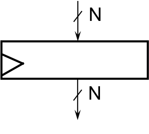 N-bit Register
Registers are denoted in our circuits by the symbol to the right; note
the annotations on the data input and output lines to show they represent
bundles of $N$ wires carrying $N$ bits simultaneously.
Adding logic to clocked devices
8.3.2. Adding logic to clocked devices
There are a variety of approaches to building complex sequential systems.
 Finite State Machine
A simple approach suggested in
Section 8.1 is to use a single multibit register
to hold the entire system state, as shown to the left.
This approach is convenient for certain sequential circuit applications, and
is the basis for the
Finite State Machine abstraction discussed in
Chapter 9.
The dynamic discipline imposed by the register in the above diagram requires
that its setup and hold time requirements, $t_{SETUP}$ and $t_{HOLD}$, be met.
Assume that the combinational logic has propagation delay $t_{PD/LOGIC}$ and contamination
delay $t_{CD/LOGIC}$, and the propagation and contamination delay specifications
for the register are $t_{PD/REG}$ and $t_{CD/REG}$ respectively.
Then the dynamic discipline requires that
- $t_{PD/REG} + t_{PD/LOGIC} + t_{SETUP}$ be less than the
clock period, to assure that the new state data will meet the register
setup time requirement;
- $t_{CD/REG} + t_{CD/LOGIC} \ge t_{HOLD}$, to assure that the register
hold time requirement is met;
- The setup time for the input data is at least $t_{PD/LOGIC}+t_{SETUP}$,
to assure that changes in input data propagate to the register in time to
meet its setup time requirement; and
- The hold time requirement for the input data is at least
$t_{HOLD} - t_{CD/LOGIC}$ to assure that input value changes conform
to the register hold time requirements.
It is often more convenient to distribute state information of a complex
system among various subsystems, allowing the construction of such systems from
sequential components.
Orderly construction of systems with distributed state -- and management of the
exploding number of consequent setup and hold time requirements -- demands
the constraints of an additional engineering discipline.
While there are several alternatives, the simplest and most common of these
is the
single clock synchronous discipline presented in
Section 8.3.3.
Single Clock Synchronous Discipline
8.3.3. Single Clock Synchronous Discipline
A straightforward approach to engineering sequential systems of arbitrary
complexity is to use a single, shared, periodic clock signal to dictate
the timing of validity for all signals within the system.
 Single Clock Synchronous System
We can build such systems from combinational logic and interspersed registers
as sketched to the right, so long as a few simple rules are followed.
The basic idea is that the active edges of a single clock signal dictates
timing of all register reloads throughout the system, and, consequently,
the timing of the validity of each register output. Each output typically
propagates through some combinational logic to another register,
where it must become valid in time to meet the target register's setup
time requirement prior to the
next active clock edge.
The clock period is then chosen to be sufficiently long to cover the
propagation delay and setup time of each such path, assuring that all
setup times within the system are met.
In general, the design of a single-clock synchronous system requires that
- Components are combinational devices and clocked devices (i.e., registers).
- The circuit contains no combinational cycles -- every cyclic directed
path must go through at least one register (or other clocked device).
- A single clock input to the system directly drives the clock input of each
clocked component; no gates or logic may be imposed on clock signals.
- Every internal path (of the form $REG_{SOURCE} \rightarrow LOGIC \rightarrow REG_{TARGET}$)
has sufficient contamination delay to cover the hold time requirement of the target register.
- The period of the system clock is sufficiently long to cover the propagation delay along
every internal path (again of the form $REG_{SOURCE} \rightarrow LOGIC \rightarrow REG_{TARGET}$)
plus the setup time of the target register.
- Each input $IN$ to the system is subject to a setup time requirement sufficiently
long to guarantee that every path of the form $IN \rightarrow LOGIC \rightarrow REG_{TARGET}$
covers the propagation delay through $LOGIC$ plus the setup time of the target register.
The tedium of meeting internal hold time requirements can be mitigated by the use
of registers whose contamination delay is at least as great as their hold time
requirement, assuring that hold times are met in each path between registers.
Setup and hold time requirements for inputs to the system are dictated by the paths connecting
the inputs to registers, and the timing of system outputs by paths between these
outputs and internal registers.
Synchronous Hierarchy
8.3.4. Synchronous Hierarchy
The single-clock synchronous discipline allows, in principle, the use of
clocked sequential subsystems as components.
Clocked components may themselves follow the single-clock discipline in their
internal construction, allowing a hierarchical approach to the design of
complex systems.
Since all of our single-clock sequential circuits are constructed from
flip flops and combinational logic, a hierarchical design can always be
"flattened" by expanding each clocked component into a network of flip flops
and logic; if the single-clock discipline is uniformly followed by each
component, the expanded network will follow that discipline as well.
In practice, however, such flattening is rarely necessary. If appropriate
setup and hold time constraints are specified for each component, it
follows that meeting these constraints assures that the setup and hold
time constraints of each internal register are met as well.
It is this property that motivates our generalization of flip flops
(or, equivalently, registers) to
clocked devices in our
single-clock rules.
Example: Sequential Circuit Timing
8.3.5. Example: Sequential Circuit Timing
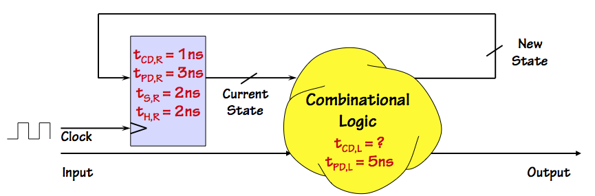 Clocked device example
Consider a clocked device constructed from a register and some combinational logic, as diagrammed to
the right. The register specifies propagation and contamination delays of 3 and 1 ns, respectively, and requires setup and hold times of 2 ns each; the combinational logic has a propagation delay of 5 ns.
We assume a periodic clock input whose active (positive) clock edges occur every $t_{CLK}$ ns.
Given these specifications, meeting the registers setup and hold times imposes the following constraints on the timing of our device:
- The feedback path from the register output through the combinational logic
to the register input must meet the 2 ns register hold time requirement.
This requires that the cumulative contamination delay around this path
$t_{CD,R}+t_{CD,L}$ be
at least 2 ns, requiring at least 1 ns of contamination delay for the combinational logic.
Unless this requirement is met, we can't expect the circuit to operate reliably.
- In order to meet the setup time requirement along this same feedback path,
the clock period $t_{CLK}$ must be long enough to include the cumulative propagation delays of the register and combinational logic as well as the specified register setup time.
Thus $t_{CLK} \ge t_{PD,R}+t_{PD,L}+t_{S,R} = 10 ns$.
The maximum clock frequency is thus $1/t_{CLK}$ or 100 MHz.
- The path from the Input through the combinational logic to the register must meet the register
setup and hold time requirements. To assure this, our device specifies required setup and hold times
for the Input line relative to active edges of the supplied clock of
$t_S = t_{PD,L}+t_{S,R} = 7ns$ and $t_H = t_{H,R} - t_{CD,L} = 1 ns$ respectively (assuming
the minimum $t_{CD,L}$ of 1 ns).
Non-CMOS Memory
8.4. Non-CMOS Memory
While the CMOS-based flip flops and registers described in section
Section 8.2 are
well suited to temporary storage of modest-sized digital values (such as state information),
other technologies are widely used for larger-scale storage requirements.
Certain of these (such as the Dynamic RAM used for computer main memory)
are
volatile, in that the information contained persists only so long
as the memory remains powered and operational. Other technologies such as magnetic
or optical disks are non-volatile, and useful for long-term and offline storage.
Most contemporary approaches to mass storage are much more sophisticated than
the glimpses given in the following sections might imply. Typically, modern
memory pushes bit storage density to the limit, and depends upon error correction
(of the sort described in
Section 3.4.3) to assure reliable storage.
RAM Arrays
8.4.1. RAM Arrays
The term
Random Access Memory or
RAM refers to a storage device architecture
containing some number of $N$-bit storage locations that are equally accessible, hence suitable
for situations in which they are accessed in random order.
Such designs are distinguished, for example from
serial-access memory devices (like
magnetic or paper tape) that prescribe a preferred order for accessing their stored data.
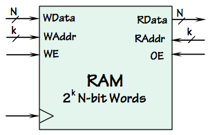 Random Access Memory
A representative model for a random-access memory component is diagrammed to the left.
It is capable of storing $2^k$ $N$-bit
words of binary data, for specified parameters
$N$ and $k$. It is organized (at least conceptually) as an array of $2^k$ locations,
each designated by an integer
address in the range $0 .. 2^k-1$.
It is typically a clocked device, hence the clock input on its lower left.
The three connections on the upper left constitute a
write port, and
consist of a $k$-bit
write address, an $N$-bit word of
write data,
and a
write enable control signal. If the write enable is asserted on an
active clock edge, the specified $N$ bits of data will be written into the location
specified by the write address.
The three connections on the upper right are a
read port, and specify
the address of an $N$-bit word to be read at the next active clock edge. The
read port may include an
output enable as shown here: a control input
that specifies whether the module is to perform a read operation and assert data
onto the
read data lines at the next active clock edge. The output enable
makes it convenient to cascade multiple RAM modules by connecting their $RData$
outputs.
RAM devices are often implemented as two-dimensional arrays of single-bit memory cells, sharing
a common addressing stucture much like that of the ROMs described in
Section 7.8.3.
Static RAM
8.4.1.1. Static RAM
Small fast memory arrays can be built entirely from CMOS gates and registers of the sort described
in
Section 8.3.1.
The design of such memory devices, however, is commonly optimized at the circuit level in ways
that violate CMOS rules in the interest of gains in performance and memory density. One such
family of memory devices are
Static RAMs or
SRAMs, named to distinguish
them from the
dynamic RAMs described in the next section.
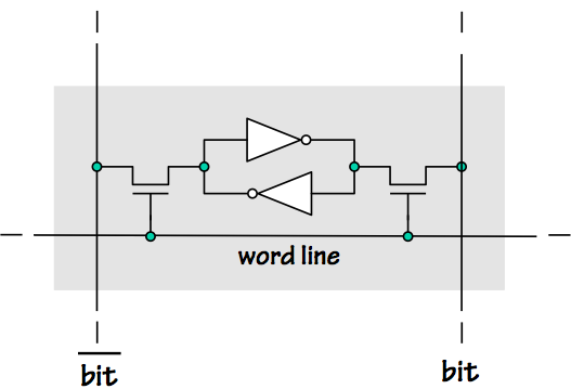 6T SRAM Cell
A typical SRAM consists of a two-dimensional array of six-transistor
cells like that shown on the right. Each row of cells shares
a
word line, asserted (driven positive) to select all cells
in that row for a read or write operation; each column shares
two
bit lines used to write or read a value to or from a cell
in a row selected by the asserted word line. Each cell consists of a
pair of cross-coupled inverters -- a simple bistable element -- whose
stored value and its complement are connected to the bit lines only
when the word line is asserted.
All cells in a row may be read by asserting the corresponding word line, driving the bit lines
of each column to voltages reflecting the 1s and 0s stored in each cell.
A cell may be written by driving the bit lines with a value and its complement, and momentarily
driving the word line. While violating CMOS rules (since opposing outputs are connected to the
same circuit node), appropriate choice of transistor sizing and drive parameters allows the
bit lines to simply overpower the value stored in the inverter pair, storing a new value.
Many variations and improvements to this SRAM cell design are possible.
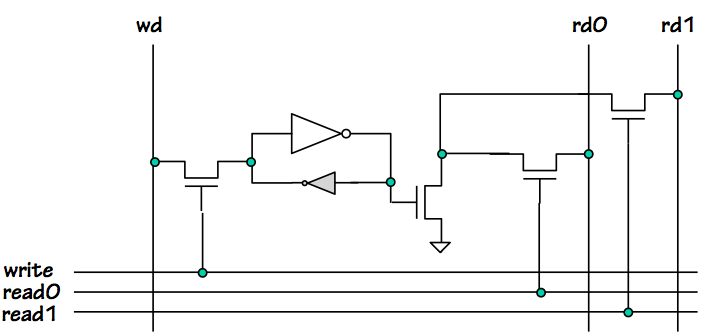 Multiport SRAM Cell
To the left is a cell for a SRAM array having two read ports and one write port, typical of the register files we will
be using in the next module of this course.
The cell uses a single bit line for a write operation; the use of assymmetric transistor sizes in the inverter pair
storing the bit allows its value to be overpowered from one end alone.
Each read port is supported by separate word and bit lines, allowing two independently-selected words to be
read simultaneously from the array during a single cycle.
Dynamic RAM
8.4.1.2. Dynamic RAM
Demand for large, cheap computer main memories has driven the development
of
Dynamic RAM or
DRAM technology to an extreme that minimizes the size of
each memory cell at the cost of sophisticated surrounding circuitry.
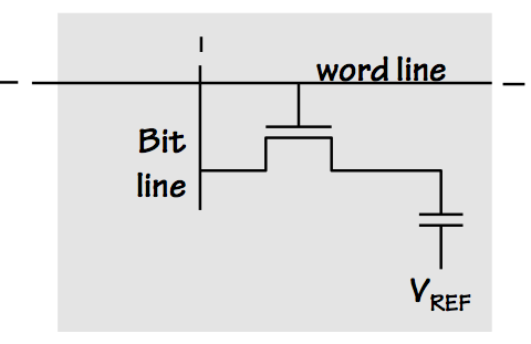 DRAM Cell
DRAM stores a single bit of information at each cell in the form of a charge on a
capacitor, using a structure like that shown to the right. The bottom terminal on the
capacitor is connected to a fixed reference voltage (such as ground), and the other terminal
is left "floating" (disconnected) so that no current flow will disturb the stored charge.
A single NFET is capable of momentarily connecting the floating end of the capacitor to a
vertical
bit line; this momentary connection is used both for setting the value
stored at the cell and reading the stored value.
The cell shown is again one of many arranged in a two-dimensional array, with vertically
aligned cells sharing a bit line and horizontal rows sharing word lines.
To store a value in a cell, the appropriate bit line is precharged to the appropriate
voltage and the voltage on the word line is raised briefly so that the NFET conducts
and charges the capacitor. Once the NFET returns to its usual non-conducting state,
the charge on the capacitor will be undisturbed by variation of the bit line voltage.
To read the value stored in the cell the word line is again asserted so that the
NFET briefly connects the bit line to the capacitor. In this case, a sensitive sense
amplifier connected to the bit line detects the effect of the connection on its voltage,
and determines whether the charge that had been stored on the capacitor represents a
zero or a one. The read operation is destructive (since it causes the stored charge
to be dissipated), so each read operation is immediately followed by a write operation
on the same cell to restore the stored information.
Because there is some leakage of the charge stored in each dynamic RAM cell, DRAMs
have to be periodically refreshed. This involves reading each cell and rewriting their
values, and leads to the "dynamic" in the name of this technology.
Magnetic and Optical Memories
8.4.2. Magnetic and Optical Memories
Mass memory technologies often involve significant mechanical components;
rotating optical and magnetic storage are popular contemporary examples.
These devices store bits as cells with persistent magnetic or optical state on a relatively
large surface, and use mechanical means to move an optical or magnetic head to
the appropriate position to read or record data. Although they can transfer
(read or write) data at high rates, they are decidedly not optimized for random
access: access to an arbitrary datum on a hard disk, for example, typically requires
a time on the order of ten milliseconds.
For this reason, rotating disk memory is typically used to access large blocks of
data stored in consecutive locations on the media.
Chapter Summary
8.5. Chapter Summary
The extension of our digital abstraction to include systems with
internal
state adds several key concepts:
- The notion that individual signal wires may contain a sequence
of potentially different logic values during the course of a
computation;
- The use of clock signals whose transitions dictate
the timing of transitions between valid logic values on signal wires;
- The need for a dynamic discipline to identify intervals
during which signal validity is guaranteed.
Because the design of basic elements with state from basic circuit
elements
is complex and error prone, we choose to carefully engineer a small
repertoire of
memory devices and restrict our design of
complex sequential systems to a mix of these and combinational devices
according to a carefully prescribed discipline. Our memory devices
include large
dynamic RAM arrays and magnetic/optical storage,
as well as
flip flops using carefully engineered feedback
loops and combinationial devices:
- A bistable latch may be constructed using a lenient
mulitplexor, and provides provably reliable storage so long as
an appropriate timing discipline is followed;
- Latches may be used to construct a flip flop, a
single-bit clocked storage device. Flip flops provide reliable
storage, again so long as an appropriate dynamic discipline is
followed.
- The dynamic discipline for clocked devices involves
- A clock signal, whose active (positive) edges
prescribes allowable times for transitions on other inputs;
- Setup and Hold times $t_s$ and $t_h$,
which establish a window surrounding each active clock transition
during which other inputs must be stable and valid; and
- Propagation and contamination delay specifications $t_{pd}$ and $t_{cd}$ on
each output, measured from the time of the active clock edge
to guarantee intervals of output validity.
- $N$ flip flops can be combined as an $N$-bit register, sharing a clock input;
- The single-clock synchronous discipline allows clocked circuit
elements to be interspersed with combinational logic, avoiding
combinational cycles and sharing a clock signal, to form new clocked components.
Although most of the systems in this subject follow the simple synchronous
single-clock discipline outlined here, there are plausible alternatives.
This subject is revisited briefly in
Section 11.8.