Combinational Logic
7. Combinational Logic
Armed with the abstract model of
combinational devices
outlined in
Chapter 5 and the concrete
implementation technology for simple gates of
Chapter 6,
we turn out attention to techniques for constructing combinational
circuits that perform arbitrarily complex useful functions.
To this end, we use the constructive property of combinational
devices outlined in
Section 5.3.2: an acyclic
circuit whose components are combinational devices is itself a
combinational device. That is, the behavior of such a circuit
can be described by the combination of a functional and timing
specification derived from the circuit topology and the component
specifications.
Functional Specifications
7.1. Functional Specifications
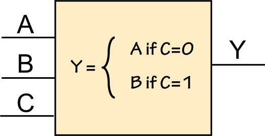
There are a variety of notations we can use to specify the functional
specification of a combinational device such as the 3-input, single-output
module shown to the right.
We might simply use a sentence or algorithmic description of each output
such as that shown in the box.
A more systematic specification is the
truth tables that have
been used in prior examples;
an equivalent truth table specification for this example is shown to the left.
A concise alternative to the truth table is a
Boolean expression:
$Y = \bar C \bar B A + \bar C B A + C B \bar A + C B A$
represents the same 3-input function as the truth table and informal
algorithmic specification.
In each case, the combinational device abstraction requires that the
functional description specify a logical ($0$ or $1$) value for each
combination of input values.
Boolean Expressions
7.2. Boolean Expressions
Boolean expressions are a ubiquitous notation in the engineering
of digital systems. They constitute a simple algebra for functions defined on
the domain of truth values ($0$ and $1$), and define three basic operations:
- Multiplication (logical AND): $A \cdot B$ or simply $A B$ represents
the logical conjunction of the values $A$ and $B$: the result is $1$
only if $A$ and $B$ are both $1$.
- Addition (logical OR): $A + B$ represents the logical disjunction
of the values $A$ and $B$; the result is $1$ if $A=1$ or $B=1$ or both.
- Negation (logical NOT or inversion): $\overline A$ represents the logical
inverse of $A$: $\overline A = 1$ if $A=0$, $\overline A = 0$ if $A = 1$.
The use of familiar algebraic notation -- multiplication and addition -- for
logical AND and OR operations takes a bit of time for the unitiated to assimilate.
The following list summarizes some properties of Boolean expressions that are
worth internalizing:
Boolean Identities
| OR rules: |
$a+1=1$ | $a+0=a$ |
|
$a+a = a$ |
| AND rules: |
$a \cdot 1=a$ | $a \cdot 0=0$ |
|
$a \cdot a = a$ |
| Commutativity: |
$a+b=b+a$ | $a \cdot b = b \cdot a$ |
| Associativity: |
$(a+b)+c=a+(b+c)$ |
|
$(a \cdot b) \cdot c = a \cdot (b \cdot c)$ |
| Distributivity: |
$a \cdot (b + c) = a \cdot b + a \cdot c$ |
|
$a+b \cdot c = (a+b)\cdot(a+c)$ |
| Complements: |
$a + \overline a = 1$ |
$a \cdot \overline a = 0$ |
|
$\overline{\overline a} = a$ |
| Absorption: |
$a + a \cdot b = a$ |
$a + \overline a \cdot b = a + b$ |
|
$a \cdot (a+b)=a$ |
$a \cdot (\overline a + b) = ab$ |
| Reduction: |
$a\cdot b + \overline a \cdot b = b$ |
$(a+b)\cdot(\overline a + b) = b$ |
DeMorgan's
Law: |
$\overline a + \overline b = \overline{a \cdot b}$ |
$\overline a \cdot \overline b = \overline{a+b}$ |
As the identities in the above table shows, there are many equivalent
ways of representing a given logic function as a Boolean expression,
and a variety of techniques for simplifying a Boolean expression or
converting it to a form that is convenient for one's purposes.
While there are many Boolean expressions that represent a given
Boolean function, there is essentially only one truth table
for each function: modulo permutation of inputs, a truth table
can be viewed as a
canonical representation.
One can verify the equivalence of two Boolean expressions with
$k$ variables by building truth tables that enumerate their values
for each of the $2^k$ combinations of variable values, and checking
that the tables are identical
Truth Table Arithmetic
7.3. Truth Table Arithmetic
The truth table for a $k$-input, single-output logic function
has $2^k$ rows, listing the single-bit output for each of the
$2^k$ potential combinations of input values. Each such $k$-input
truth table has the identical form: input values are listed, conventionally
in a systematic order corresponding to binary counting order;
truth tables for different $k$-input functions thus differ only in
the $2^k$ single-bit values in their output column.
There is a one-to-one correspondence between these truth tables
and the set of $k$-input logic functions. As there are $2^k$ output
bits that distinguish a particular $k$-input function, and each
output bit may be $0$ or $1$, it follows that the total number of
possible $k$-input functions is just $2^{2^k}$ -- precisely the
number of distinct $k$-input truth tables.
There are, for example, a total of $2^{2^2} = 16$ 2-input functions,
whose truth tables are summarized below:
Note that the full set of 2-input functions includes degenerate cases
of functions whose output is independent of one or both input values.
It is worth noting that, of these sixteen 2-input functions, only six
can be implemented directly as single CMOS gates: NOR(A,B)=$\overline{A+B}$
and NAND(A,B)=$\overline{A \cdot B}$, as well
as the degnerate cases $\overline A$, $\overline B$, $0$, and $1$.
Other 2-input functions must be synthesized using multiple CMOS gates
in a combinational circuit.
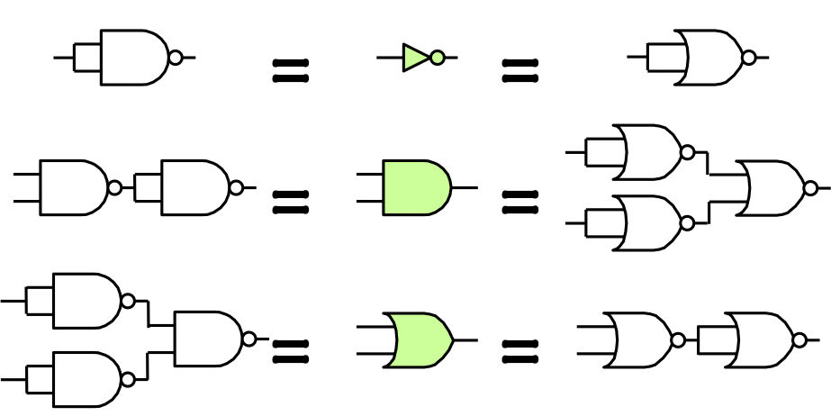
Gates and Gate Symbols
7.4. Gates and Gate Symbols
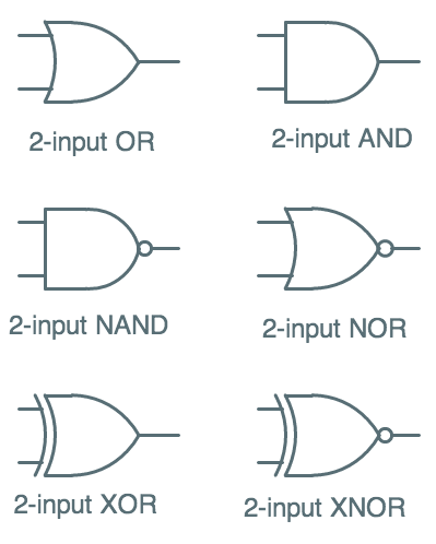 2-input gate symbols
Circuit symbols for commonly-used 2-input combinational logic components
are shown to the right; some of these (NAND and NOR) we've already seen
in connection with their direct implementation as CMOS gates. The others
require multiple CMOS gates to implement.
The 2-input AND of $A$ and $B$ can be easily implented as a NAND gate followed
by an inverter, since $A \cdot B = \overline{\overline{A \cdot B}} = \overline{NAND(A,B)}$;
similarly, OR can be implemented as a CMOS NOR gate followed by an inverter.
The more complex $XOR(A,B) = A \cdot \overline{B} + \overline{A} \cdot B$
requires several CMOS gates to implement, as does its inverse $XNOR(A,B)$.
Note the consistent use of small circles --
"inversion bubbles" --
to indicate inversion of logic levels.
Universal Gates
7.5. Universal Gates
Although there are $2^k$ $k$-input logic functions we may wish to implement
as combinational devices, the ability to synthesize new devices as acyclic
circuits implies that we can begin with a small repertoire of basic gates
and design circuits using them to build arbitrary functionality. Indeed,
the observation that Boolean expressions are built using only three operations
(AND, OR, and NOT) implies that a starting toolkit containing only AND,
OR, and inverter modules is sufficient. Moreover, since we can synthesize
$k$-input AND and OR devices from circuits of 2-input gates, it follows that
an unlimited supply of 2-input AND and OR devices, along with inverters,
will allow us to
synthesize any logic functions we might wish. We term such a set
universal,
in that it contains all we need to implement arbitrary logic functions.
Happily, the 2-input NAND and NOR operations that are easily implemented
as single CMOS gates are each, in isolation, universal.
 NAND, NOR Universality
Given the universality of the ${AND, OR, NOT}$ set,
We can demonstrate the universality of ${NAND}$ or ${NOR}$ by showing
how to implement each of ${AND, OR, NOT}$ using only NAND or NOR gates,
as shown to the right.
From a logical standpoint, this implies that arbitrarily complex combinational
systems can be built from a parts inventory containing only 2-input NAND or NOR
gates.
Sum-of-Products Synthesis
7.6. Sum-of-Products Synthesis
It is straightforward to convert a truth table to an equivalent Boolean
expression in
sum-of-products form.
Such an expression takes the form of the Boolean sum (OR) of several
terms, each of which is the product of some set of (possibly inverted)
input variables.
Each such term $t_i$ corresponds to a line of the truth
table for which the output column contains $1$ -- called an
implicant
of the function, since $t_i = 1$
implies that the output is $1$.
If we reconsider the prior 3-input example, we note that the
four $1$s in the output column imply that the output $Y$ is $1$ for each of the input
combinations $ABC = 001, 011, 110, 111$.
For each of these, we construct an implicant term that is $1$ for precisely
the specified combination of input values, by including each input variable
in the term and inverting it (via the overbar notation) if its value is
$0$. The resulting sum-of-products expression is
$\bar C \bar B A + \bar C B A + C B \bar A + C B A$, an expression whose value is $1$
for precisely those combinations of input values for which the truth table specifies
$Y=1$.
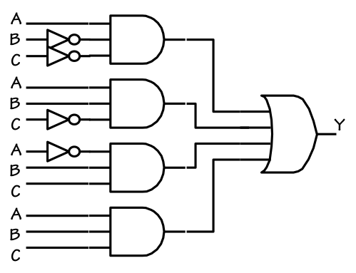 SOP Implementation
Given that Boolean expressions are built from using AND, OR, and NOT (inversion)
operations, it is tempting to synthesize circuits from Boolean expressions directly
using AND gates, OR gates, and inverters, as shown to the left.
Note that this approach generalizes to a systematic 3-tier structure
for arbitrary $k$-input functions:
- a layer of inverters to generate the necessary inverted inputs;
- A set of $N$ $k$-input AND-gates, where $N$ is the number of implicants.
Each AND gate computes the value of one term (implicant) of the sum-of-products
expression; and
- An $N$-input OR gate to sum the terms.
Although the direct sum-of-products implementation seems a straightforward
approach to implementation of arbitrary Boolean functions, it is rarely the
fastest or most efficient (in terms, say, of transistor count) of the
possible CMOS implementation techniques. This stems primarily from two
factors:
- CMOS gates are naturally inverting: AND and OR gates
use more transistors than NAND and NOR gates; optimized CMOS
implementations exploit the simpler inverting logic for circuit
simplicity, which is often at odds with the conceptual simplicity
of Boolean expressions built from AND/OR/NOT operations.
- Many Boolean functions have internal structure that can be
exploited to reduce implementation complexity, even using direct
AND/OR/NOT implementations. Such structure can often be
uncovered by manipulation of a Boolean expression to yield
a simpler, equivalent expression.
Tne number of transistors used in the above SOP implementation gives
a rough proxy for its implementation cost. Our example uses four
inverters (at two transistors each), four 3-input AND gates each
requiring 8 transistors, and one 4-input OR requiring 10 transistors.
The total transistor count for this circuit is thus 50; we will see
shortly that the same function can be implemented far more cheaply.
Boolean Simplification
7.6.1. Boolean Simplification
Although a direct sum-of-products representation for a Boolean function is
easy to derive systematically from a truth table, it rarely represents
the function's simplest or most convenient form.
We often can simplify the sum-of-product expressions by algebraic
manipulation, using the identites of
Section 7.2 and
other tools.
Consider, for example, the unsimplified Boolean expression for the
3-input function of the previous sections:
$Y = \bar C \bar B A + \bar C B A + C B \bar A + C B A$
Although this structure of the SOP implementation shown above
corresponds directly to the structure of this circuit, we can
find simpler expressions that suggest correspondingly simpler
implementations of the same function by algebraic manipulation
using the identities given above.
A particularly useful identity is the
reduction identity
$a \cdot b + a \cdot \bar b$, which generalizes to:
$\alpha X \beta + \alpha \bar X \beta= \alpha \beta$
where $\alpha$ and $\beta$ are arbitrary (possibly empty) Boolean subexpressions.
Thus we can simplify a Boolean expression by looking for pairs of terms that are identical
except for some variable $X$, which is inverted in one term but not in the other, and
by replacing the pair of terms by a single simpler term which omits the variable
that omits $X$.
Applying this reduction step to the 3-input Boolean expression above,
we notice that the terms $C B \bar A$ and $C B A$ match the pattern
and can be replaced by the simpler term $C B$, yielding
$Y = \bar C \bar B A + C B + \bar C B A$
Noticing that $\bar C \bar B A$ and $\bar C B A$ can be reduced
to $\bar C A$, we simply further to
$Y = \bar C A + C B$
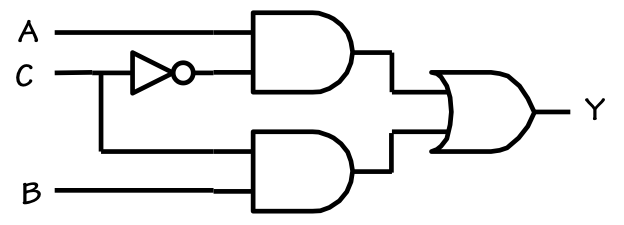 Simplified SOP circuit
which is a simpler sum-of-products Boolean equation that is
equivalent to our original 4-term unreduced equation.
In fact it has two implicants rather than four
and each implicant is simpler, involving two variables rather than three.
Each of the terms of this expression implies a $1$ for
two input
combinations, allowing us to use fewer implicants in our simplified
expression. In fact each term of the simplified expression is a
prime implicant, meaning that no it is not subsumed by
any other (yet simpler) implicant for the function.
In addition to suggesting simpler implementations, the simplified expression
makes the function easier to understand: quick inspection reveals that $Y=A$
when $C=0$, but $Y=B$ when $C=1$. Although this characterization applies
equally to the equivalent 4-term unsimplified expression, that relationship
is much less obvious.
Based on this simplified Boolean expression, the direct sum-of-products
implementation shown to the right is correspondingly less complex
than that of our unsimplified 4-term SOP expression.
This implementation uses a single inverter (2 transistors), two
2-input ANDs (6 transistors each) and a single 2-input OR (6 transistors)
for a total transistor count of 20.
Repeated application of reduction steps together with other basic
identities (such as reordering variables in a term to recognise
reduction opportunities) is the approach taken by most software tools
for Boolean simplification.
Pushing Bubbles
7.6.2. Pushing Bubbles
Another of the Boolean identities listed in
Section 7.2 is
often referred to as
DeMargan's Law, and constitutes a useful
tool for transformation of Boolean expressions to more useful forms.
One statement of Demorgan's law is
$\overline A + \overline B = \overline{A \cdot B} = NAND(A,B)$:
that is, an OR with inverted inputs computes precisely the same value as an AND with
an inverted output. Conversely, it follows that
$NOR(A,B) = \overline{A + B} = \overline{A} \cdot \overline{B}$.
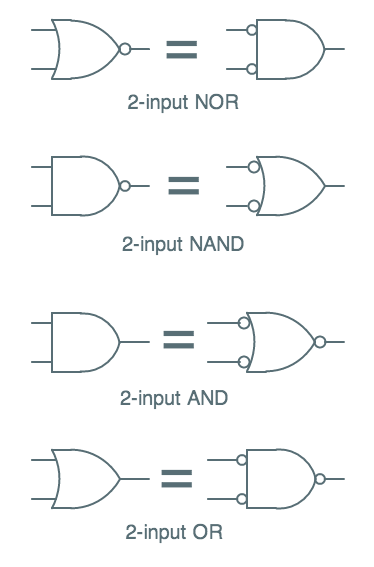 Demorganized gate symbols
It is sometimes useful to reflect these equivalences in logic circuits
by using
"DeMorganized versions of circuit symbols, such as those
shown to the left.
Note that each row of the table shows two different circuit symbols
that perform the identical logic function -- indeed, they represent
precisely the same circuit implementation.
In each case, the two symbols reflect an application of DeMorgan's law:
inverting each input and output of an AND operation to convert it to
an OR (since $A \cdot B = \overline{\overline{A}+\overline{B}}$) or
inverting each input and output of an OR operation to convert it to
an AND (since $A + B = \overline{\overline{A} \cdot \overline{B}}$).
By judicious use of these equivalences we often can replace conceptual AND and OR operations
by the cheaper and faster NAND and NOR operations prefered in our
CMOS technology. The use of alternative symbols (together with our
understanding that pairs of inversion bubbles on the same wire cancel
each other) can make such transformations easier to recognise in our
circuit diagrams.
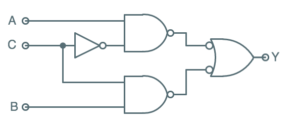 NAND-NAND SOP circuit
The diagram to the right shows a NAND/NAND implementation of the simplified
sum-of-products expression that has been our running example. Relative to
the AND/OR implementation, we have replace AND gates by NANDs (saving 2
transistors each) and used a Demorganized NAND gate instead of an OR
to add the terms (saving another 2 transistors). The total transistor count
of this implementation is 14.
Of course, it computes the same value $Y = \bar C A + C B$ as our original
50-transistor circuit.
Circuit Timing
7.7. Circuit Timing
As noted in
Section 6.4.4, we can bound the timing specifications
$t_{PD}$ and $t_{CD}$ of an acyclic circuit of combinational components by
considering cumulative delays along each input-to-output path through the
circuit.
| Device | $t_{PD}$ | $t_{CD}$ |
|---|
| Inverter | 2ns | 1ns |
| NAND | 3ns | 1ns |
| Circuit | 8ns | 2ns |
To illustrate, consider our 3-input NAND-NAND circuit implemented using
CMOS gates whose timing specifications are summarized to the left.
We may bound the propagation delay by the longest cumulative $t_{PD}$
along any input-output path; in this case, the constraining path involves
an inverter and two NAND gates for a total propagation delay of 8ns.
Similarly, we bound the contamination delay by the shortest cumulative
$t_{CD}$ along any input-output path, in this case involving 2 NAND
gates for a total contamination delay of 2ns.
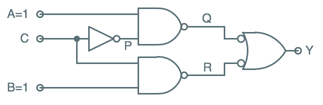 NAND-NAND Circuit Signals
To explore the detailed timing of signals flowing through the circuit as the
result of an input change, consider an experiment where the $A$ and $B$ inputs
of our circuit are held to $1$ for an interval that includes a $1 \rightarrow 0$
transition on the $C$ input.
The diagram to the right includes new labels $P$, $Q$, and $R$ attached to internal
nodes of the circuit.
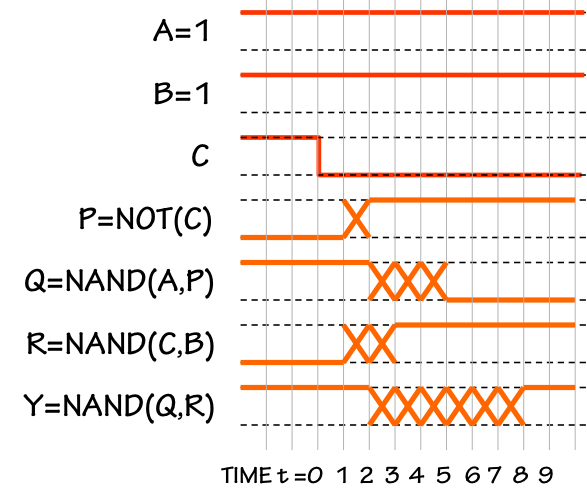 Signal Timing
The diagram to the left details the timing of each signal in the circuit
as we maintain $A=B=1$ and apply an instantaneous $1 \rightarrow 0$ transition
on $C$ at time $t=0$.
Note that, prior to the $C$ transition, $A=B=C=1$ and all signals in the
circuit are at stable, valid values; the output $Y=1$, as dictated by
the functional specification of the circuit.
The $1 \rightarrow 0$ transition on $C$ at $t=0$ stimulates the propagation of
signal changes through the circuit, eventually affecting the output.
It is worth diving into the details of the timing of this signal flow
to understand the guarantees provided by the (lenient) CMOS gates in
our circuit:
- The inverter output $P$ remains $0$ for 1ns, due to the $t_{CD}=1ns$
inverter specification. It becomes a valid $1$ at $t=2$ -- 2ns following
the input transition -- as guaranteed by the inverter's $t_{PD}=2$ specification.
Note that during the intervening 1ns interval, the signal on $P$ is
unspecified -- it may be a valid $0$, a valid $1$, or invalid.
This interval of undetermined logic value is shown on the diagram by
a crosshatched X pattern.
- The output $R$ of the lower NAND gate remains $0$ for the 1ns NAND $t_{CD}$,
and becomes a valid $1$ after the 3ns NAND $t_{PD}$, with an intervening
2ns period of unspecified (possibly invalid) value.
- The output $Q$ of the upper NAND gate doesn't see an input change until
$t=1$, when its $P$ input becomes invalid. $Q$ remains a valid $1$ for an
additional 1ns contamination delay, after which it is contaminated.
$Q$ becomes a valid $0$ at $t=5$, the earliest time at which its inputs
have been valid for the 3ns NAND propagation delay.
- The output gate sees $R$ go invalid at $t=1$, but maintains a valid
$Y=1$ output for its 1ns contamination delay. Its $R$ input becomes a
valid $1$ at $t=3$, but its $Q$ input remains invalid until becoming
$0$ at $t=5$. Since a single $1$ input is not sufficient to determine
the output of even a lenient NAND gate, the output $Y$ cannot be
assumed to be valid until the 3ns propagation delay after both inputs
become valid. Thus, $Y=1$ at $t=8$, following a 6ns interval of unspecified
output value.
It is reassuring that, as the timing diagram shows, the output $Y$
remains valid for 2ns following the input transition and becomes
valid 8ns after that transition; this is consistent with the circuit's
$t_{CD}$ and $t_{PD}$ bounds computed earlier.
It may be bothersome, however, that the output of our circuit is unspecified
for an interval between the two periods of valid $1$s.
Given that $A=B=1$, the transition on $C$ does not affect the value of
$Y = \bar C A + C B$, and we might ask that the output remain a valid $1$
during this transition.
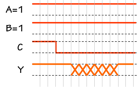 Non-lenient behavior
During the unspecified period, however, the output of our non-lenient
device may become a valid $0$, or even vacillate
between $0$ and $1$ several times, before settling back to its final value
of $1$.
Such anomalies are often referred to as
glitches or
hazards.
The fact that the use of lenient components does not guarantee
lenience of acyclic circuits built from them is annoying, but usually
not problematic.
In fact this device is a valid combinational device (for which
any
input change contaminates the output value for a propagation delay) but
not a
lenient combinational device (whose output remains valid
despite changes in irrelevent inputs).
For reasons explored in the next Chapter, reliable digital systems
require a timing discipline that makes signal values significant only
during prescribed intervals, allowing transient periods of invalidity
during which they may make transitions. A simple such discipline
is described in
Section 8.3.3.
Lenient Circuits
7.7.1. Lenient Circuits
In certain important applications, however, lenience of a combinational
component is critical. Suppose we had an application that requires
a
lenient device that computes $Y = \bar C A + C B$?
We know that single CMOS gates are lenient, but a bit of analysis
convinces us that this function cannot be implemented as a single
CMOS gate; hence we must resort to a circuit of CMOS components.
Fortunately, it is possible -- at some additional engineering and
hardware cost -- to design acyclic circuits of lenient components
that are themselves lenient combinational devices.
In general, non-lenience of combinational circuits stems from
the dependence of an output on any of several input-output propagation
paths. In the case of our 3-input NAND-NAND circuit, observe
that for $C=1$ the path holding the output $Y=1$ involves circuit
nodes $C=1 \rightarrow R=0 \rightarrow Y = 1$; when $C=0$,
the alternative path $C=0 \rightarrow P=1 \rightarrow Q=0 \rightarrow Y=1$
forces the output to be $1$.
Following the $1 \rightarrow 0$ transition of $C$, the former path
is disabled (no longer forcing $Y=1$) and the latter path is enabled
(forcing $Y=1$), but the timing of these two events is not strictly
controlled. Hence there is a period during which neither path may
be active, and the value of $Y$ is hence undetermined.
Using the terminology of
Section 7.6,
our circuit computes the value $Y = \bar C A + C B$ via two
implicants,
$C A$ and $\bar C B$, computed by separate paths and combined in the
final logical OR (using a Demorganized NAND).
The $C$ transistion switches responsibility for holding $Y=1$ from one
path to the other, effectivly selecting whether the $A$ input or the $B$
input should be taken as the output value $Y$. In our test case,
$A=B=1$ rendering the output value independent of which path is
selected;
however, there is no single path in our circuit which forces $Y=1$
when $A=B=1$.
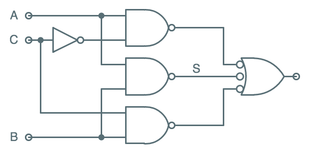 Lenient NAND-NAND Circuit
We can address this problem by adding a path representing a third
implicant, $A B$, to the circuit. The circuit shown to the right
uses three NAND gates to compute inverted versions of the three
implicants $A \bar C$, $A B$, and $C B$, and the final 3-input
NAND computes their sum. The resulting value is $Y = A \bar C + A B + C B$,
which is logically equivalent to our simplified $Y = A \bar C + C B$;
however, now there is a path dedicated to ensuring $Y=1$ for each
of three (rather than two) implicants.
This approach can be generalized to the implementation
of lenient combinationial circuits to compute arbitrary
Boolean expressions.
In the general case, a sum-of-products implementation using
lenient components will be lenient if it includes logic representing
every
prime implicant of the function.
Fan-In and Delay
7.7.2. Fan-In and Delay
Although the CMOS gate examples have focused on 2-input NAND and NOR
gates, we can of course implement many functions with more inputs --
higher
fan-in -- as single CMOS gates.
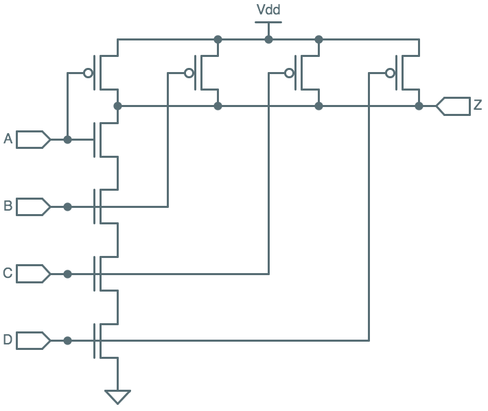 4-input NAND gate
For example, the diagram on the right shows the straightforward extension of our CMOS NAND
gate to 4 inputs, by including additional PFETs and NFETs gated by the new inputs to the
parallel and series chains of the pullup and pulldown circuits.
While this approach can in theory be extended to single CMOS gates of arbitrarily many inputs,
the performance of CMOS gates degrades with increasing fan-in due to electrical loading.
In practice, it is typically preferable to implement functions of more than about four
inputs as circuits of smaller gates.
Certain common logical functions like AND, OR, and XOR offer a variety of
alternative approaches to large-fan-in circuit design. Each of these functions $F$
have the property that $F(a_1,...,a_k) = F(a_1, F(a_2, ..., a_k))$, suggesting
a strategy for repeatedly using 2-input gates to reduce the fan-in requirement by one.
But we may also observe that for each such function $F$,
$F(a_1,...,a_k) = F(F(a_1, ..., a_j), F(a_{j+1}, ..., a_k))$: we may partition
the $k$ arguments into multiple sub-operations, and employ a divide-and-conquer
approach to their combination.
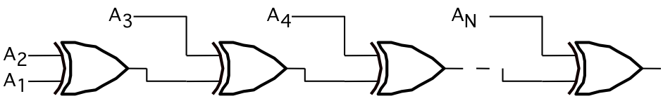
 2-input XOR
Suppose, for example, we have a 2-input XOR gate shown on the left.
Note from the truth table that the XOR function has the value $1$ if and only if
an
odd number of its inputs are $1$, a function that extends in a
straightforward way to arbitrarily many inputs and that has the properties
described for $F$ above. We desire to implement $XOR(a_1, ..., a_N)$ for
arbitrary fan-in, a function that returns $1$ if the number of $1$s among its $N$
inputs is odd. This function, sometimes called
odd parity, is useful
for error detection techniques such as those discussed in
Section 3.4.
The observation that
$XOR(a_1,...,a_k) = XOR(a_1, XOR(a_2, ..., a_k))$
suggests that we can compute $XOR(a_1, ..., a_N)$ by the circuit shown to
the right, in which each of the two-input XOR gates combines a single
input with the cumulative XORs from the gates to its left.
While this circuit works correctly, we note that the longest input-output
path goes through all $N-1$ of the component 2-input gates, yielding a
propagation delay that grows in proportion to the number of inputs.
While this may be an acceptable approach in some circumstances, we often
prefer an approach that minimizes the worst-case propagation delay of the
resulting circuit.
For
associative operations like $XOR$, we observe that
$XOR(a_1,...,a_k) = XOR(XOR(a_1, ..., a_j), XOR(a_{j+1}, ..., a_k))$
suggesting that we can reduce our $N$-input XOR to the XOR of the result
of two $N/2$-input XORs -- a step that halves the fan-in at the cost of
a single gate delay.
Repeated application of this divide-and-conquer step results in a
binary tree
structure as shown to the left. Note that a tree having $k$ levels of 2-input
components has a propagation delay proportional to $k$, but provides a fan-in
of $2^k$ inputs.
Thus an $N$-input XOR, for large fan-in $N$ can be computed by the tree
in time proportional to $log_2(N)$, an improvement over the linear
delay of the preceding approach.
Similar tree structures can be used to compute many other functions
whose extension to $N$ arguments is straightforward, including AND, OR,
and addition. Certain functions (like NAND and NOR) admit tree implementations,
but require some care due to their special properties (e.g., inversion).
Other functions don't decompose so nicely, and don't lend themselves
to tree implementations; an example is the $N$-input
majority
function, which returns $1$ if a majority of its inputs are $1$.
Systematic Implementation Techniques
7.8. Systematic Implementation Techniques
Typically the smallest, fastest, and most cost-effective implementation
of a complex Boolean function is a custom circuit designed and optimized
to compute that function. While there are many sophisticated techniques
and tools for designing such circuits, the customization process is
inherently expensive -- both in engineering and manufacturing costs.
For this reason, several synthesis approaches have been developed that
forego function-specific optimizations in order to allow the straightforward
implementation of an arbitrary $k$-input Boolean function by parameterizing
a fixed, function-generic hardware substrate. In this section we sample
several such approaches.
Multiplexors
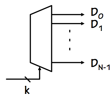
7.8.1. Multiplexors
The three-input Boolean function used as a running example in this Chapter is
a a commonly-used component in our combinational repertoire: a 2-way
multiplexor
(or
Mux in the vernacular of logic design).
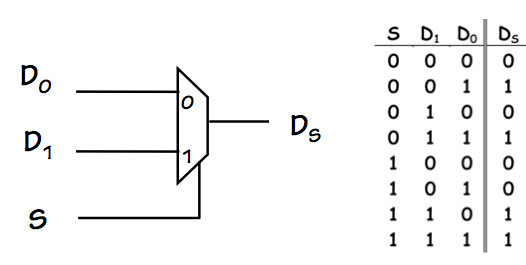 2-way Multiplexor
The logic symbol and truth table for a 2-way mux is shown to the right.
A useful model for its behavior is a 2-way logic-controlled switch:
it takes 2 independent data inputs $D_0$ and $D_1$, as well as a
select
input $S$; its output (after a propagation delay) is $D_0$ if $S=0$ or $D_1$ if $S=1$.
Muxes are useful for routing the flow of data through our combinational circuits
on the basis of
control signals applied to their select inputs; we will
see many examples of such uses in subsequent chapters.
As discussed in previous sections of this Chapter, the implementation of a multiplexor
may or may not be lenient; the example of section
Section 7.7.1 is,
in fact, a lenient 2-way multiplexor.
This device plays a key role in the implementation of memory devices in the next Chapter.
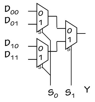
 4-way Multiplexor
The multiplexor function can be generalized to $2^k$ inputs and $k$ select lines;
the diagram to the left shows a 4-way multiplexor, whose output is one of the four
data inputs as selected by the four possible combinations of inputs on the two
select lines.
One way to implement a $2^k$-way multiplexor is to use a 2-way mux
selecting among the output of two $2^{k-1}$-way muxes, as illustrated
in the 4-way mux implementation shown to the right.
Lookup Table Synthesis
7.8.2. Lookup Table Synthesis
The ability of a multiplexor to select one of $2^k$ input values suggests
its use as a mechanism to perform
table lookup functions: based
on its select input, its output is one of the connected data values.
 Mux-based NAND
We might implement an arbitrary 2-input Boolean function, for example, by
use of a 4-way mux as shown to the left.
The Boolean inputs drive the select lines, and hence select one of the
four data inputs. If we connect the data inputs to constant $0$ and $1$
values corresponding to the output column of the Boolean function's
truth table, the supplied select inputs will effectively look up
the correct output from the supplied values. The function "programmed"
into this implementation is NAND, but by simply changing the constant values --
$0$s and $1$s implemented via
$V_{DD}$ and ground connections --
we can make this circuit compute any of the 16 2-input Boolean functions.
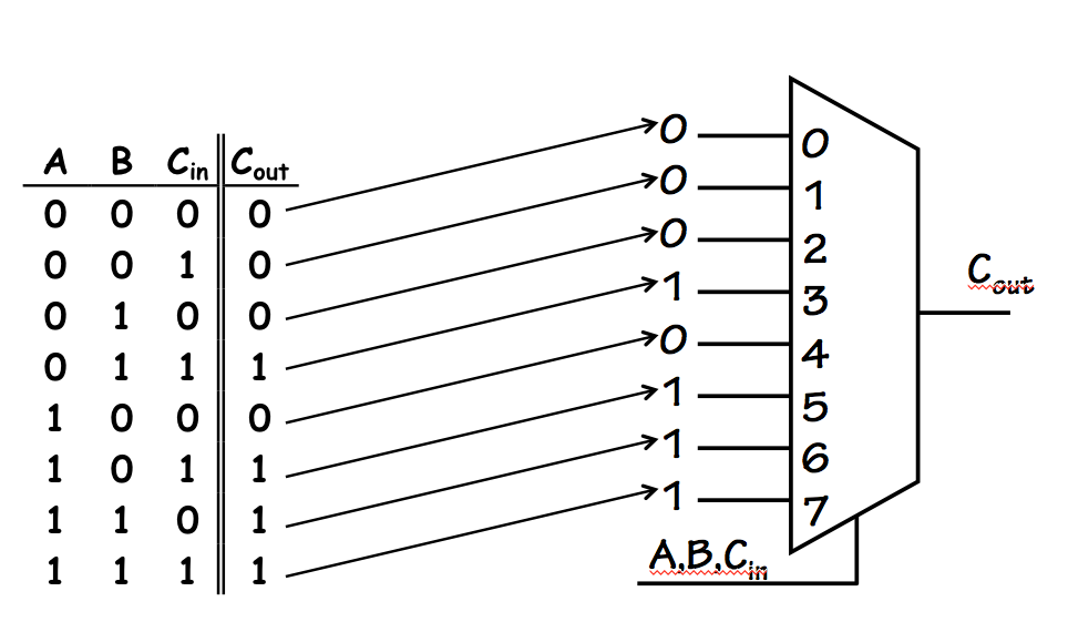 3-input table lookup
Using larger multiplexors, we can implement functions with more inputs.
The diagram to the right shows the implementation of a 3-input function -- the
carry output for a 1-bit
full adder device -- using an 8-way
multiplexor. Again, the mux simply chooses among the constant values
supplied (in accordance with a truth table) as its data inputs.
Table lookup approaches are attractive in applications where it is desirable
to isolate the hardware structure from the choice of the function to be implemented,
for example when that function might be frequently changed or is specified as
a customization parameter of an otherwise commodity hardware device.
Read-only Memories
7.8.3. Read-only Memories
When the number of inputs becomes large, the use of a simple mux-based approach
to table lookup is tedious: a 10-input function, for example, requires a 1024-way
multiplexor.
For this reason, table lookup approaches have evolved to space-efficient structures
that more effectively exploit the 2-dimensional layout constraints of the surface
of a silicon chip.
Such approaches are often called
read-only memories (ROMs),
and share with the mux-based lookup table the fact that the output
values are
programmed into the structure as data values
in locations corresponding to combinations of inputs. The various
input combinations may be viewed as
addresses of memory locations,
and the data values as the memory
contents.
This section provides a glimpse of a simple read-only memory technology
for the systematic implementation of arbitrary Boolean functions.
Although the technology is compatible with CMOS logic, it is noteworthy
that it differs from CMOS gate implementation in a number of important
ways -- among them are lenience and power consumption characteristics.
Decoders
7.8.3.1. Decoders
In order to expand our table lookup implementation to two dimensions, we
introduce another building block: a $2^k$-way
decoder.
 Decoder
The circuit symbol for a decoder is shown to the right.
It takes as input $k$ select lines, whose values select one of
$2^k$ output lines to be driven to a logical $1$; all unselected lines
remain at a logical $0$. Thus for any combination of valid inputs,
one and only one of the output lines will be $1$: the output lines
may be viewed a
decoded (or "
one-hot") representation
of the binary value supplied on the $k$ select inputs.
ROM-based Full Adder
7.8.3.2. ROM-based Full Adder
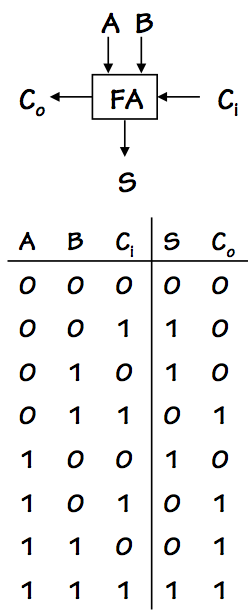 Full Adder
Consider the simple 3-input, 2-output combinational device whose symbol and
truth table are shown to the left.
The device is in fact a 1-bit
full adder, a building block used
in the constuction of binary adders in subsequent chapters; for now, we
use it simply as an example of combinational functions we might wish to
implement.
The device takes three binary inputs $A$, $B$, and $C_i$ and produces the
two outputs $S$ and $C_o$. Note that we could have split this into two
separate 3-input devices for computing $S$ and $C_o$ respectively;
however, their combination as a single device allows us to exploit some
shared logic for implementation efficiency.
In particular, we will use a single decoder to convert the three input bits
to a more convenient form: a logic $1$ on exactly one of its eight outputs.
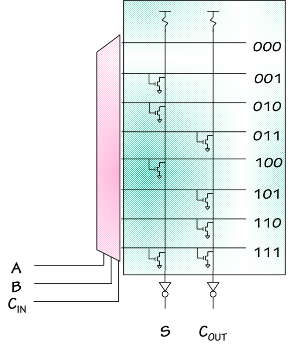 ROM-based Full Adder
One approach to the ROM-based full adder is shown to the right.
The three inputs are decoded to drive exactly one of the eight horizontal
lines to $1$; the selected line corresponds to the row of the truth table
selected by the current inputs, or one possible product term in a sum-of-products
expression.
Superimposed over the horizontal decoder outputs are two vertical lines,
each connected to $V_{DD}$ through a resistive pullup. This passive pullup
serves to cause the voltage on each vertical line to have a default value
of $1$.
At each of the intersections between a horizontal decoder output and a vertical
line, there is either no connection or an NFET pulldown.
The presence of a pulldown at an intersection causes a $1$ on the horizontal
line to force the vertical line to $0$, by overpowering the passive resistive
pullup.
Thus each of the vertical lines performs a logical NOR function of the
horizontal lines for which there are pulldowns; an inverter between each
vertical line and the $S$ and $C_o$ outputs causes each output to be a
logical OR of the decoder outputs selected by the presence of pulldowns.
Comparing the diagram with the truth table for the full adder, note that
there are pulldowns at precisely those intersections corresponding to $1$s
in the truth table output columns. Thus the logical function that appears
at each output corresponds to the sum-of-products computation of the functions
represented in the table.
ROM Folding
7.8.3.3. ROM Folding
Although this ROM implementation exploits a second dimension to compute multiple
outputs from a single decoded set of inputs, its vertical dimension still grows
in proportion to $2^k$ where $k$ is the number of inputs.
In general, long lines cause delays; we would prefer to make the ROM array more
nearly square by using a greater number of shorter vertical lines.
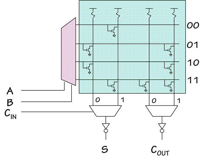 Folded ROM
Fortunately, this is a fairly straightforward engineering tradeoff.
On the left is shown a revised ROM layout, in which two of the inputs
($A$ and $B$) are decoded onto four horizontal lines rather than the previous eight.
Each output is then computed by two vertical lines, one giving the value for $C_i=0$
and another for $C_i=1$; the $C_i$ input is used in an output multiplexor
for each output to select the proper value.
Commodity/Customization Tradeoffs
7.9. Commodity/Customization Tradeoffs
The design approach taken by ROMs, involving a regular array of
cells sharing the same internal structure, is used in other systematic
logic technologies as well.
These include read-write memories (RAMs) as well as several varieties
of logic arrays.
These approaches exemplify a recurring technology tradeoff between the advantages of
an application-generic, mass-produced commodity implementation and an
application-specific implementation highly optimized around the structure
of a particular solution.
An attractive feature of ROMs and other commoditized approaches is that
nearly all of the structure of a given-size ROM is independent of the
actual function it performs: the customization may be left to a final
parameterization step (adding a metal layer to a chip, or even field
programming in the case of
flash memories or FPGA logic arrays).
Chapter Summary
7.10. Chapter Summary
Having moved from transistors into the logic domain, we face the task
of combining logic elements to synthesize higher-level logical functions.
Techniques explored include:
- While truth tables are an effective tool for the specification
of logic functions, Boolean expressions are often a convenient
alternative. Familiarity with identities and Boolean manipulation
techniques is an important skill for the logic designer.
- Any truth table can easily be translated to a sum-of-products (SOP)
Boolean expression, which can be mechanically converted to a 3-level
gate implementation of the function.
Useful SOP techniques include NAND-NAND and NOR-NOR implementations.
- SOP implementations are not necessarily minimal; function-specific
structure may often be exploited to implement a given function using
fewer CMOS devices.
- Multiplexors are useful building blocks, and can be used to
systematically implement arbitrary functions as lookup tables.
- ROMs generalize this table-lookup implementation approach,
offering a fixed hardware complexity independently of the truth
table details.