
Circuits
4. Circuits
Digital systems can be built using a variety of underlying physical technologies: mechanical, chemical, biological, hydraulic, and many others. While many of the lessons of this subject apply to systems built using any physical mechanism, we focus on electronics as our implementation medium. The success of electronics in this (and many other applications) rests on one of the most successful abstractions in the history of engineering: the electronic circuit. In this chapter, we explore the circuit as an abstraction, and review some of its properties as well as its limitations for our purposes.The Circuit Abstraction
4.1. The Circuit Abstraction
A triumph of classical physics is the articulation of Maxwell's equations, shown to the right, which concisely capture the fundamental relationship between electric and magnetic fields.
\begin{equation}
\begin{array}{rcl}
\nabla\cdot{\bf D} & = & \rho \\
\nabla\cdot{\bf B} & = & 0 \\
\nabla\times{\bf E} & = & - { {\partial{\bf B}}\over{\partial t} } \\
\nabla\times{\bf H} & = & {\bf J} + { {\partial{\bf D} }\over{\partial t} }
\end{array}
\label{eq:maxwell}
\end{equation}
Maxwell's Equations
If these equations don't make much sense to you, don't fret:
a powerful engineering abstraction offers us ordinary engineers
a vastly less complex model, allowing us to design useful electronic systems
using simple rules and building blocks. That model is the
lumped-element circuit.
Maxwell's equations are admirable for their generality: they apply
to arbitrary configurations of continuous 3-space, having arbitrary
distributions of physical properties such as electrical conductivity.
They consolidate scientific breakthroughs by Faraday, Ampere, Gauss,
and other stalwarts of science, and represent a major component of our
understanding of classical physics.
As a design space for engineering useful systems, however, they
leave much to be desired:
their generality, a source of power as a scientific model, gives
little guidance to the engineer with a specific problem to solve.
The Lumped-element Circuit
4.2. The Lumped-element Circuit
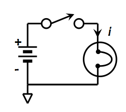
The key to reducing the unconstrained 3-dimensional universe described by Maxwell's Equations to a tractable design space for engineering is to restrict our attention to a tiny subset of possible physical configurations. In particular, instead of considering arbitrary three-dimensional configurations of materials with arbitrary electrical properties, our simplified model considers only finite configurations of discrete components from a small repertoire, electrically isolated from each other except for specific connections made by ideal, perfectly conducting wires. In this model a circuit is analyzed in terms of voltages and currents, rather than the underlying electric and magnetic fields. A circuit consists of a finite number of components, each having one or more terminals or ports. The ports are connected to equipotential nodes, each consisting of a connected set of ideal wires; at any time, each node carries a single voltage to every port it connects. Current flowing into and out of ports is defined by each component specification in terms of the applied voltages. The constraints of Maxwell's equations are simplified to Kirchoff's laws:- The sum of all currents entering each node is zero.
- The directed sum of the voltage differences around a cycle is zero.
| Component | Symbol |
|---|---|
| Battery | 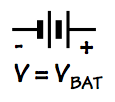 |
| switch |  |
| lamp |  |
| ground |  |
Linear Circuits
4.3. Linear Circuits
It is often useful to view a circuit as taking a time-varying signal -- e.g., a voltage waveform -- applied to some input node, and responding via another time varying signal at an output node. In this view, a circuit C transforms an input waveform given by some time-varying function $f(t)$ into an output waveform $g(t)$; more concisely, $C(f(t)) = g(t)$. The important special case of linear circuits has the property that, for every linear circuit $C$, if $C(f_1(t))=g_1(t)$ and $C(f_2(t))=g_2(t)$ then $C(f_1(t)+f_2(t)) = g_1(t)+g_2(t)$. Linear circuits have been extensively studied, and there is a powerful set of engineering tools for analyzing their behavior, Although for the construction of digital systems our primary technology is nonlinear circuits, an intuitive appreciation of basic linear components is useful for modeling electrical issues in real-world systems, and understanding the limits of the circuit model.| Component | Symbol | v/i constraint |
|---|---|---|
| Resistor |  |
$v = R \cdot i$ |
| Capacitor | 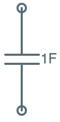 |
$i = C\cdot {dv \over dt}$ |
| Inductor |  |
$v = L\cdot {di \over dt}$ |
| Voltage Source |
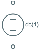 |
$v = fn(t)$ |
Parasitic RLC elements
4.3.1. Parasitic RLC elements
The set of components in a circuit implies a set of equations dictating constraints on the voltages and currents throughout that circuit, and analysis of the circuit's behavior typically involves solving these equations. In circuits involving capacitors and inductors, the equations involve derivatives, leading to differential equations to be solved. While the time-domain analysis of arbitrary linear circuits is beyond the scope of this subject, a modest intuitive appreciation of the behavior of linear elements is useful to understand the impact of parasitic resistances, inductances, and capacitances that inevitably creep into the digital circuits we will build.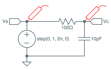
RC Circuit
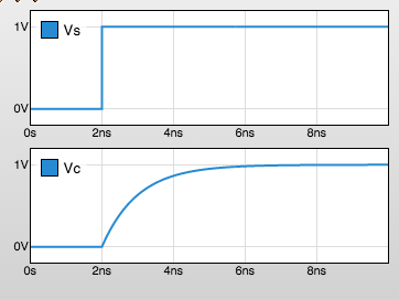
RC Circuit Analysis
Power and Energy
4.3.2. Power and Energy
The instaneous power, in watts, flowing into or out of a two-terminal device is $P = I\cdot V$, where $I$ is the current flowing through the device and $V$ is the voltage drop across its terminals. Power is a measure of the rate of flow of energy; one watt of power corresponds to a flow rate of one joule of energy per second. In some applications, power may be viewed as an asset: if we were building machines to do mechanical work or cook pizza, we might try to maximize power parameters. In machines designed to process information, however, we usually seek to minimize power flow; power represents energy consumption, and power dissipation generates heat which must be removed by cooling apparatus. In modern computing circuitry, energy consumption has emerged as one of the major bottlenecks among the cost/performance tradeoffs faced by the engineer. Among our linear circuit elements, the resistor dissipates power by turning it into heat, a form of energy that is unrecoverable for further use by our circuits. Modern digital circuits tend to avoid resistors to minimize their consequent ohmic losses: a voltage drop of $V_R$ across an $R$-ohm resistor causes a current $I_R={V_R \over R}$ and, by Ohm's law, a power dissipation of ${V_R}^2\over R$. Even when we avoid deliberate incorporation of resistors in our digital designs, parasitic resistances (e.g. of wires) dissipate power through ohmic losses wherever current flows in our circuits. The so-called reactive linear components, capacitors and inductors, do not dissipate power in our circuit model. Rather, the $V\cdot I$ energy pumped in or out of them effects the storage of energy within the device, in the form of an electric (capacitor) or magnetic (inductor) field. The energy stored in a $C$-farad capacitor charged to a voltage of $V$ is ${C\cdot V^2}/2$; the energy stored in an $L$-henry inductor carrying a current $I$ is ${L\cdot I^2}/2$. Although this energy is stored rather than dissipated, in simple digital circuits it is ultimately consumed by ohmic losses in parasitic resistances and consequently wasted. The stored energy is, however, in theory recoverable; and clever circuit designs ("charge recovery circuits") attempt to minimize power dissipation by recycling some of the stored energy.Analog video toolkit
4.4. Analog video toolkit
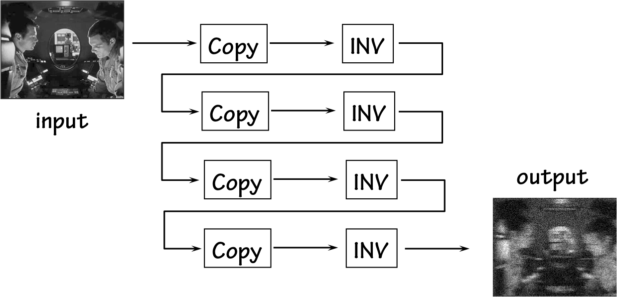
The productivity of engineering within a particular application domain is enhanced by building a repertoire of reusable building blocks -- a toolkit of generally useful modules for that domain. Ideally, there is a simple, easy to understand conceptual model underlying the toolkit: modules can be plugged together simply to make systems that behave in predictable and useful ways. The design of such toolkits, and their simplicity and coherence, often involves conventions for representing domain-specific information communicated between connected modules of a system. Consider, for example, a toolkit involving modules for the processing of streams of video, using a plausible "analog" scheme for encoding monochrome video as a continuous voltage waveform. We begin by choosing a convention for encoding the intensity of a single point in an image -- say, 0 volts for black, 1.0 volts for white, and any voltage between 0 and 1 volt to represent the corresponding intermediate shade of gray.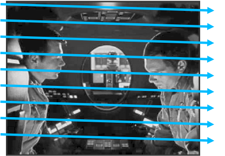
Raster Scan
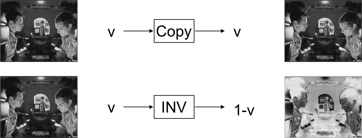
Video Operators
Analog Video System
Circuit model limitations
4.5. Circuit model limitations
The lumped-element circuit model, and its extension to digital circuits introduced in Chapter 5, represent powerful engineering abstractions responsible for much of our technological progress during recent decades. However, the circumspect circuit designer is keenly aware of physical realities that are ignored by the circuit model in the interests of design simplicity, and adopts engineering disciplines carefully designed to deal with these limitations of the model. In this section, we briefly discuss two classes of circuit model limitations and ways in which we will accommodate them in our engineering practice.Noise Sources
4.5.1. Noise Sources
The first class of circuit model limitations stems from the fact that circuit element specifications represent idealized behavior that can only be approximated by our real-world circuits. Discrepancies between actual and ideal circuit behavior that fall into this category include- Parisitic resistance, inductance, capacitance, stemming from our inability to tease these electrical effects apart as cleanly as our circuit model dictates;
- Imprecision in parametric values of real-world components, due to manufacturing variations and allowable tolerances;
- Environmental effects such as external magnetic and electric fields, temperature variation, etc.
Wire Delays
4.5.2. Wire Delays
A more serious limitation of the circuit model is the fact that it is oblivious to the physical notion of space. A ten-mile wire has the same circuit-theoretic properties as a one-micron wire: it has a single potential, which can change instaneously and synchronously over its entire length. We recognize that this model is physically unrealistic for a variety of reasons. Firstly, instantaneous discontinuities in voltage and current are infeasible due to parasitic capacitative and inductive effects: an instantaneous change would require an infinite voltage and/or current spike. But more importantly, we know that a signal takes finite time to propagate from one physical location to another: physics places an inviolable upper bound -- the speed of light -- on signal propagation, and under practical circumstances the effective bound is lower. While the speed of light seems (and is) a generous speed limit for signal propagation, its not infinite. Indeed, the speed of light is on the order of one foot per nanosecond; in the era of high-speed computing, a nanosecond has become a long time. Historically, the space-oblivious circuit model arose under circumstances where devices were slow relative to signal propagation over the distances involved, and this relation still applies in many applications (such as the flashlight of Section 4.2). However, the assumption of negligible signal transit time is much less applicable to modern, high-speed digital circuits, causing a real tension between the circuit model and our engineering needs.Output Loading
4.5.2.1. Output Loading
This tension results in large part from our desire to concisely and locally characterize the behavior of system components, as we did with those of our video toolkit of Section 4.4. We would like, for example, the device specifications to include the timing and values of voltages on the output terminals of a device, and allow the engineer to assume that these are the values and timing that will be seen at inputs connected to these terminals. Unfortunately, the real-world implementation of our device does not have absolute control over the voltage on an output terminal: its actual voltage and timing depends on the loading imposed by the connected circuitry. Worse, that loading includes parasitic effects that depend on the length and routing of connected wires, details that are typically determined very late in the design process. Our very real dilemma is this: we'd like to give our engineers the Tinkertoy-set simplicity of modules that completely specify their outputs in terms of their inputs. However, physical realities dictate that some aspects of our inputs will be determined by factors (output loading and wire routing) external to the modules, and unknown at the time in the design process when the device is selected. Fortunately, there is an imperfect but tolerable compromise we can use to address this dilemma. Our tecnology of choice for digital circuits -- CMOS, detailed in Chapter 6 -- has properties that allow us to model the effects of output loading as a simple (unknown) additional delay applied to signals at component output terminals. We can exploit this feature of our technology by the following system design approach:- devise an engineering discipline (and associated circuit technology) by which we build sytems with a single system-wide parameter -- clock period -- which dictates both the performance of the system and timing allowed for signals at every node in our circuit.
- specify the voltage and timing at component outputs assuming a light load, ignoring additional load-dependent delays.
- Design each system using the optimistic timing of device specifications, understanding that the actual system will run somewhat slower than calculated due to unaccounted-for wire delays. Given the engineering discipline of 1. above, we are assured that for some clock period, the system as designed will work properly.
- Once a system design is complete, route the wires (a CPU-intensive process) and analyze the actual loading on each circuit node. We use this data to determine the actual clock period (and hence performance) of our system.
Chapter Summary
4.6. Chapter Summary
The lumped-element circuit is a major engineering abstraction: it reduces the vastly complex range of possible physical systems to a simple, tractible set of functional special cases. Noteworthy points:- A circuit consistes of a finite number of circuit elements, each with finitely many terminals;
- Terminals are interconnected via a finite number of equipotential circuit nodes;
- Manufacturable devices provide good approximations of circuit elements and wires provide good approximations of equipotential nodes, under many circumstances; BUT
- The circuit-theoretic ideal ignores inevitable real-world issues such as wire delay, parasitics, and noise.