
32-bit ALU
When entering numeric values in the answer fields, you can use integers (1000, 0x3E8, 0b1111101000), floating-point numbers (1000.0), scientific notation (1e3), engineering scale factors (1K), or numeric expressions (3*300 + 100). Useful links: Problem 1. Design Problem: 32-bit Arithmetic and Logic Unit See the instructions below. Use the Jade instance below to enter your design. To complete this design problem, select the /alu/alu module and click in the Jade toolbar and the built-in tester will either report any discrepencies between the expected and actual outputs, or, if your design is correct, it will record the test passed.- design for maximum performance (minimum latency)
- design for minimum cost (minimum area)
- design for the best cost/performance ratio (minimize area*latency)
inverter, buffers, tristate driver
2-, 3- and 4-input AND, OR, NAND and NOR gates
2-input XOR and XNOR gates
2:1 and 4:1 multiplexors
D-register and D-latches
2-, 3- and 4-input AND, OR, NAND and NOR gates
2-input XOR and XNOR gates
2:1 and 4:1 multiplexors
D-register and D-latches
See the library documentation for details on the appropriate connections for each gate. In Jade, the gates in the standard cell library can be found in the parts bin under "/gates/".
Since we're designing at the gate level we can use a faster simulator that only knows about gates and logic values (instead of transistors and voltages). Note that your design can't contain any mosfets, resistors, capacitors, etc.; the gate-level simulator only supports the gate primitives in the standard cell library. Inputs are still specified in terms of voltages (to maintain netlist compatability with the other simulators) but the gate-level simulator converts voltages into one of three possible logic values using the vil and vih thresholds specified at the beginning of your design file:
0 logic low (voltages less than or equal to vil threshold)
1 logic high (voltages greater than or equal to vih threshold)
X unknown or undefined (voltages between the thresholds, or unknown voltages)
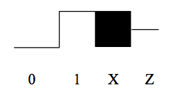
A fourth value "Z" is used to represent the value of nodes that
aren't being driven by any gate output (e.g., the outputs of tristate
drivers that aren't enabled). The following diagram shows how these
values appear on the waveform display:
1 logic high (voltages greater than or equal to vih threshold)
X unknown or undefined (voltages between the thresholds, or unknown voltages)
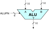 The 32-bit ALU we will build will be a component in the Beta
processor we will address in subsequent laboratories. The logic
symbol for our ALU is shown to the right. It is a combinational
circuit taking two 32-bit data words A and B as inputs, and producing
a 32-bit output Y by performing a specified arithmetic or logical
function on the A and B inputs. The particular function to be
performed is specified by a 6-bit control input, FN, whose value
encodes the function according to the following table:
The 32-bit ALU we will build will be a component in the Beta
processor we will address in subsequent laboratories. The logic
symbol for our ALU is shown to the right. It is a combinational
circuit taking two 32-bit data words A and B as inputs, and producing
a 32-bit output Y by performing a specified arithmetic or logical
function on the A and B inputs. The particular function to be
performed is specified by a 6-bit control input, FN, whose value
encodes the function according to the following table:
| FN[5:0] | Operation | Output value Y[31:0] |
|---|---|---|
| 00-011 | CMPEQ | Y = (A == B) |
| 00-101 | CMPLT | Y = (A < B) |
| 00-111 | CMPLE | Y = (A ≤ B) |
| 01---0 | 32-bit ADD | Y = A + B |
| 01---1 | 32-bit SUBTRACT | Y = A - B |
| 10abcd | Bit-wise Boolean | Y[i] = Fabcd(A[i],B[i]) |
| 11--00 | Logical Shift left (SHL) | Y = A << B |
| 11--01 | Logical Shift right (SHR) | Y = A >> B |
| 11--11 | Arithmetic Shift right (SRA) | Y = A >> B (sign extended) |
| Bi | Ai | Yi |
| 0 | 0 | d |
| 0 | 1 | c |
| 1 | 0 | b |
| 1 | 1 | a |
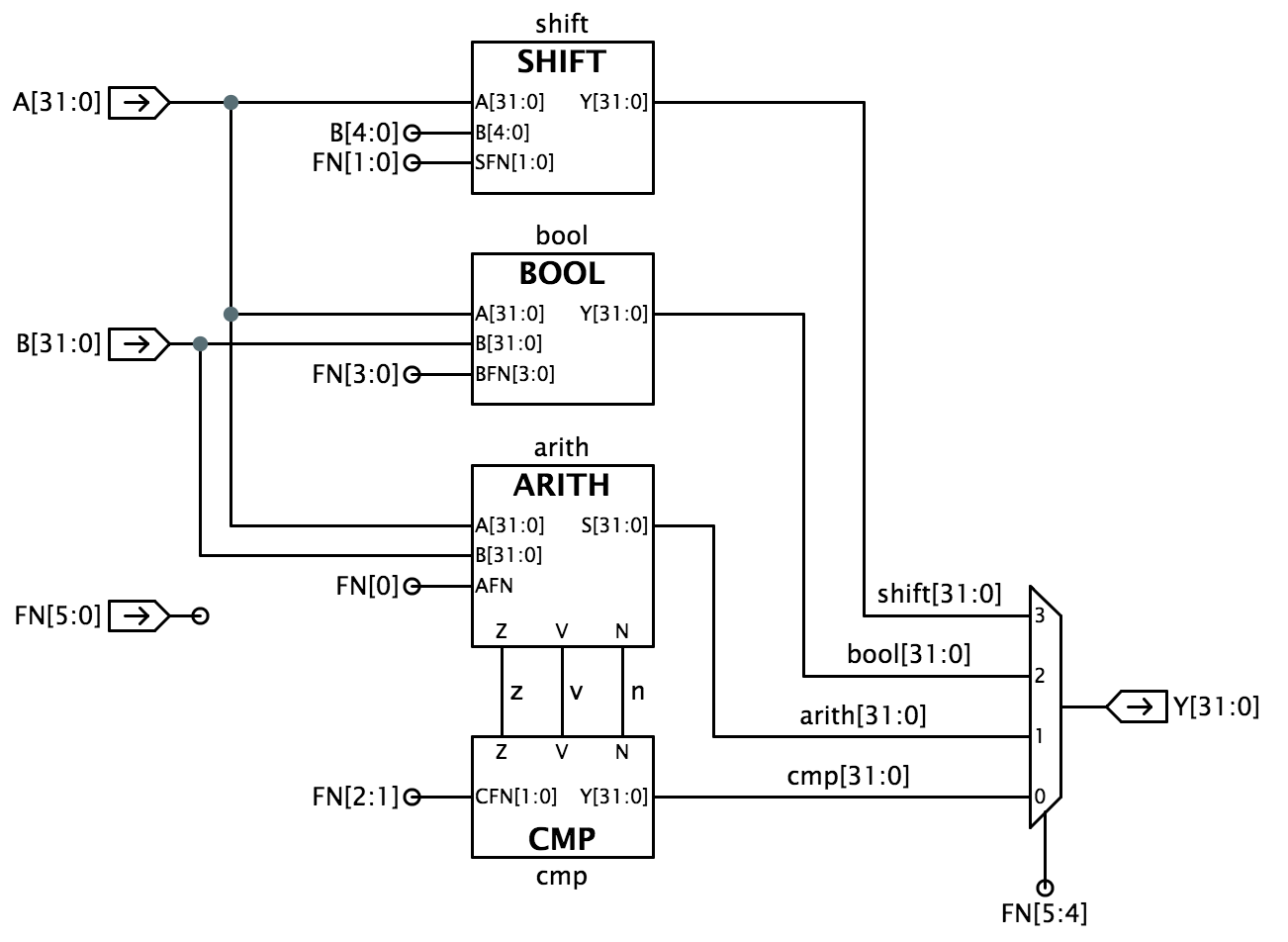
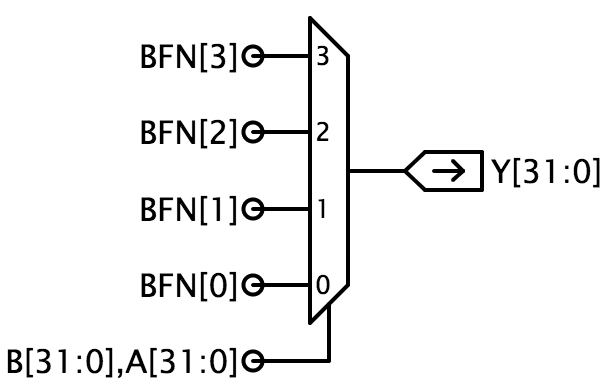 The suggested implementation uses 32 copies of a 4-to-1
multiplexor (mux4) where BFN[3:0] encode the operation to
be performed and A[31:0] and B[31:0] are hooked to the multiplexor's select
inputs. This implementation can produce any of the 16 2-input Boolean
functions.
The suggested implementation uses 32 copies of a 4-to-1
multiplexor (mux4) where BFN[3:0] encode the operation to
be performed and A[31:0] and B[31:0] are hooked to the multiplexor's select
inputs. This implementation can produce any of the 16 2-input Boolean
functions.
Hint: Jade will automatically replicate a logic gate to match the width of
the gate's inputs and outputs to the width of the signals that connect
to the gate.
For example, the MUX4 gate shown above has a 1-bit output signal,
which in this schematic is hooked to Y[31:0], a signal of width 32.
So Jade will replicate the MUX4 32 times, the output of the first MUX4
connects to Y[31], the output of the second MUX4 connects to Y[30],
and so on.
The input signals are then replicated (if necessary) to provide
the inputs for each of the 32 MUX4 gates.
Each MUX4 gate requires 2 select signals, which are
taken from the 64 signals provided. B[31] and A[31] connect to the select lines of the first
MUX4, B[30] and A[30] connect to the select lines of the second MUX4,
and so on.
Each MUX4 gate requires 4 data signals. The specified BFN inputs
are only 1 bit wide, so the specified signals are each replicated 32
times, e.g., BFN[0] is used as the D0 input for each of the 32 MUX4s.
The following table shows the encodings for some of the BFN[3:0]
control signals used by the test jig (and in our typical Beta
implementations):
| Operation | BFN[3:0] |
|---|---|
| AND | 1000 |
| OR | 1110 |
| XOR | 0110 |
| "A" | 1010 |
Hint: What do I do when the verification fails?
The failure notification will tell you which signal failed
verification and the simulated time at which the mismatch between the
actual value and expected occurred. The tests are actually a sequence
of 100ns testing cycles and the reported time will be at the
end of one of the cycles when the output values are checked for
correctness.
Move your mouse over the plot of the appropriate signal waveform
until the vertical time cursor is approximately at the failure time.
Then double-click to zoom in on the plots around that particular time;
zoom in enough so that all the signals for that testing cycle are
readable. Now you can figure out what the circuit was being asked to
do for that particular test and, hopefully, deduce why your circuit is
producing an incorrect output.
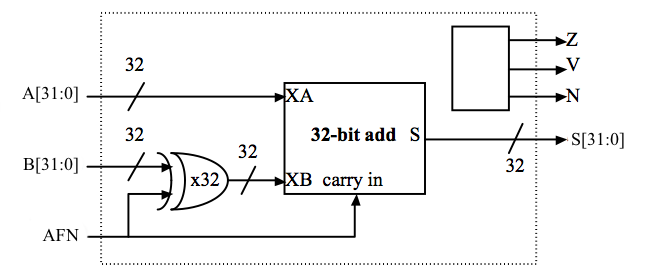
ARITH unit
Design an adder/subtractor (ARITH) unit that operates on 32-bit
two's complement inputs and generates a 32-bit output. It will be
useful to generate three other output signals to be used by the CMP
unit: Z which is true when the S outputs are all
zero, V which is true when the addition operation overflows
(i.e., the result is too large to be represented in 32 bits),
and N which is true when the sum is negative (i.e., S[31] = 1).
Overflow can never occur when the two operands to the addition have
different signs; if the two operands have the same sign, then overflow
can be detected if the sign of the result differs from the sign of the
operands:
| Comparison | Equation for LSB | CFN[1:0] |
|---|---|---|
| A = B | LSB = \(Z\) | 01 |
| A < B | LSB = \(N \oplus V\) | 10 |
| A ≤ B | LSB = \(Z + (N \oplus V)\) | 11 |
| Operation | SFN[1:0] |
|---|---|
| SHL (shift left) | 00 |
| SHR (shift right) | 01 |
| SRA (shift right with sign extension ) | 11 |
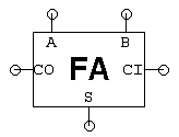
- A single test vector for the full adder consists of 3 input
values (one each for A, B and CI) and 2 output values (S and CO).
To run a test the input values from the current test vector are
applied to the device under test and then the actual output values
are compared against the expected values listed by the test
vector. This process is repeated until all the test vectors have
been used. Assuming we know nothing about the internal circuitry
of the full adder, how many test vectors would we need to
exhaustively test its functionality?
- Consider a 32-bit adder with 64 inputs (two 32-bit input operands,
assume CIN is tied to ground as shown in the diagram below)
and 32 outputs (the 32-bit result). Assume we don't know anything
about the internal circuitry and so can't rule out the possibility
that it might get the wrong answer for any particular combination
of inputs. In other words, just because the adder got the correct
answer for 2 + 3 doesn't allow us to draw any conclusions about
what answer it would get for 2 + 7. If we could apply one test
vector every 100ns, how long would it take to exhaustively test
the adder?
- Clearly, testing a 32-bit adder by trying all combinations of
input values isn't a good plan!
Shown below is a schematic for a 32-bit ripple-carry adder.
 Except for the carry-in from the bit to the right, each bit of
the adder operates independently. We can use this observation to
test the adder bit-by-bit and with a bit of thought we can
actually run many of these tests in parallel. In this case the
fact that the adder got the correct answer for 2 + 3 actually
tells us a lot about the answer it will get for 2 + 7. Since the
computation done by adder bits 0 and 1 is the same in both cases, if
the answer for 2 + 3 is correct, the low-order two bits of the
answer for 2 + 7 will also be correct.
So our plan for testing the ripple-carry adder is to test each
full adder independently. When testing bit N we can set A[N] and
B[N] directly from the test vector. It takes a bit more work to
set CI[N] to a particular value, but we can do it with the correct
choices for A[N-1] and B[N-1].
If we want to set CI[N] to 0, what values should A[N-1] and B[N-1]
be set to? If we want to set CI[N] to 1? Assume that we can't
assume anything about the value of CI[N-1].
Except for the carry-in from the bit to the right, each bit of
the adder operates independently. We can use this observation to
test the adder bit-by-bit and with a bit of thought we can
actually run many of these tests in parallel. In this case the
fact that the adder got the correct answer for 2 + 3 actually
tells us a lot about the answer it will get for 2 + 7. Since the
computation done by adder bits 0 and 1 is the same in both cases, if
the answer for 2 + 3 is correct, the low-order two bits of the
answer for 2 + 7 will also be correct.
So our plan for testing the ripple-carry adder is to test each
full adder independently. When testing bit N we can set A[N] and
B[N] directly from the test vector. It takes a bit more work to
set CI[N] to a particular value, but we can do it with the correct
choices for A[N-1] and B[N-1].
If we want to set CI[N] to 0, what values should A[N-1] and B[N-1]
be set to? If we want to set CI[N] to 1? Assume that we can't
assume anything about the value of CI[N-1].
bits 0, 2, ... bits 1, 3, ... A[31:0] B[31:0] A=0, B=0, CI=0 A=0, B=0, CI=0 0x00000000 0x00000000 A=1, B=0, CI=0 A=0, B=0, CI=0 0x55555555 0x00000000 A=0, B=1, CI=0 A=0, B=0, CI=0 0x00000000 0x55555555 A=1, B=1, CI=0 A=0, B=0, CI=1 0x55555555 0x55555555 A=0, B=0, CI=0 A=1, B=0, CI=0 0xAAAAAAAA 0x00000000 A=0, B=0, CI=0 A=0, B=1, CI=0 0x00000000 0xAAAAAAAA A=0, B=0, CI=1 A=1, B=1, CI=0 0xAAAAAAAA 0xAAAAAAAA A=1, B=0, CI=1 A=1, B=0, CI=1 0xFFFFFFFF 0x00000001 A=0, B=1, CI=1 A=0, B=1, CI=1 0x00000001 0xFFFFFFFF A=1, B=1, CI=1 A=1, B=1, CI=1 0xFFFFFFFF 0xFFFFFFFF - Three of the compare unit's inputs (Z, V and N) come from the adder/subtractor running in subtract mode computing A-B:
Z = 1 if A-B is 0
N = 1 if A-B is negative (OUT[31] = 1)
V = 1 if there's been an overflow. The ALU, which only has
an adder, computes A-B as A+(-B) = A+(~B)+1. Let XB = ~B, the
bit-wise complement of B. An overflow occurs if the sign
of the result (OUT[31]) differs from the signs of the adder's operands
(A[31], XB[31]). Note that if the signs of A and XB differ, the
addition cannot produce an overflow.
To test the compare
unit, we'll need to pick operands for the adder/subtractor that
generate all possible combinations of Z, V and N. It's easy to
see that any combination with Z = 1 and N = 1 is not possible
(the output of the adder cannot be negative and zero at the same
time!). It also turns out that combinations with Z = 1 and V =
1 cannot be produced by a subtract operation.
For each of the combinations of Z, V and N shown below,
choose the subtraction operation that will produce the specified
combination of condition codes.
Problem 3. The Versatile BOOL unit
As we saw in the instructions for the ALU,
the bitwise Boolean operations are specified by FN[5:4]=10. In this
case, the remaining FN bits abcd are taken as
entries in the truth table describing how each bit of Y is determined
by the corresponding bits of A and B, as shown to the right.
For each of the Boolean operations \(F(A,B)\) specified below, determine
the settings for FN[3:0] so that the Bool unit will compute
desired operation.
| Bi | Ai | Yi |
| 0 | 0 | d |
| 0 | 1 | c |
| 1 | 0 | b |
| 1 | 1 | a |