Your exercise answers are saved by the browser in local storage
associated with this webpage. You can use the buttons below
to load/save the answers on your system.
Save all answers:
Load all answers (this will overwrite any answers currently saved by the browser):
Authored by Chris Terman
CMOS Adder
When entering numeric values in the answer fields, you can use
integers (1000, 0x3E8, 0b1111101000), floating-point numbers
(1000.0), scientific notation (1e3), engineering scale factors
(1K), or numeric expressions (3*300 + 100).
Useful links:
The following questions are multiple-choice. You can, of
course, simply keep guessing until you get the right answer. But
you'll be in a much better position to take the quizzes if you take
the time to actually figure out the answers.
If we set the inputs of a particular CMOS gate to voltages that
correspond to valid logic levels, we would expect the static
power dissipation of the gate to be
essentially zero depends on whether output voltage is low or high unknown with the facts given
Measuring a particular CMOS device G, we find 1.5V noise margins.
If the width of all mosfets inside of G were doubled, we
would expect the noise margins of the new gate to
stay about the same increase noticeably decrease noticeably change noticeably, but can't tell which way
To decrease the output rise time of a CMOS gate one could
increase the length of all pfets increase the width of all pfets increase the length of all nfets increase the width of all nfets none of the above
The Boolean function F(A,B,C,D) of four inputs is implemented
as a single CMOS gate whose output connects to a pullup circuit
containing only PFETs and a pulldown containing only NFETs. The output
of F is known to depend on its inputs; i.e., F(A,B,C,D) is zero for
certain input combinations and one for others. What can you deduce
about F(1,1,1,1)?
0 1 can't tell
Problem 2. Power dissipation
Almost all of the power dissipated by CMOS circuits goes into charging
and discharging nodal capacitances. This power can be computed as
\(CV^2F\) where \(C\) is the capacitance being
switched, \(V\) is the change in voltage, and \(F\) is the
frequency at which the switching happens. In CMOS circuits, nodes
are switched between ground (0 volts) and the power supply voltage
(\(V_{DD}\) volts), so \(V\) is either +\(V_{DD}\) (for a 0→1 output transition)
or \(-V_{DD}\) (for a 1→0 output transition) and so
\(V^2 = V_{DD}^2\).
Suppose we have a device implemented in a technology where \(V_{DD}\) = 5V.
If we have the option of reimplementing the device in a technology
where \(V_{DD} = 3.3V\), what sort of speedup (i.e., change in F) could
be specified for the reimplementation
assuming we want to keep the power budget unchanged?
±5%
Problem 3. CMOS logic gates
As we saw in lecture, there are 16 possible 2-input combinational
logic gates. The cost of implementing these gates varies
dramatically, requiring somewhere between 0 and 10 mosfets depending
on the gate. For example, it takes 2 mosfets to implement
"F = NOT A", but 4 mosfets (organized as two inverters) to
implement "F = A".
For each of the 2-input gates whose Karnaugh maps are given
below, indicate the minimum number of mosfets required to implement
the gate. You should only consider static fully-complementary
circuits like those shown in lecture; these implementations meet the
following criteria:
no static power dissipation
\(V_{OL} = 0V\), \(V_{OH}\) = power supply voltage
NFETs appear only in pulldown circuits, PFETs appear only in pullup circuits
the pullup and pulldown are complementary, i.e., when one path is "on", the other is "off"
the pullup and pulldown circuits can be decomposed into series and parallel connections of mosfets
all gate implementations restore incoming logic levels (so a wire connecting an input terminal to an output terminal would not be a legal gate implementation)
Hint: see the Design Problem below.
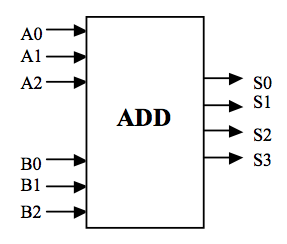
Problem 4. Design Problem: 3-bit adder
Your mission is to design and test a CMOS circuit that
performs addition of two two's-complement 3-bit numbers, producing a 4-bit
result:
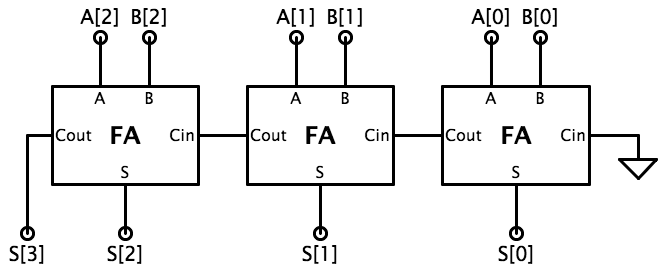
Ripple-carry adders
Let's start with a simple ripple-carry adder based on the
full-adder module, which has 3 inputs (\(A\), \(B\) and \(C_{IN}\))
and 2 outputs (\(S\) and \(C_{OUT}\)). The full adder computes the
sum of \(A\), \(B\) and \(C_{IN}\) and outputs the 2-bit answer on
\(C_{OUT}\) and \(S\). The logic equations and truth table for \(S\)
and \(C_{OUT}\) are shown below.
$$S = A \oplus B \oplus C_{IN} \qquad C_{OUT}=A\cdot B + A\cdot C_{IN} + B\cdot C_{IN}$$
\(A\)
\(B\)
\(C_{IN}\)
\(S\)
\(C_{OUT}\)
0
0
0
0
0
0
0
1
1
0
0
1
0
1
0
0
1
1
0
1
1
0
0
1
0
1
0
1
0
1
1
1
0
0
1
1
1
1
1
1
A ripple-carry adder is simply a chain of full adder modules that compute
the sum bit-by-bit, like so:
There are three goals for your implementation. First, of course,
is computing the right outputs. The other two goals involve some
engineering tradeoffs: small circuit size, as measured by the total
number of mosfets, and fast performance, as measured by the
\(t_{PD}\) of the ADDER3 circuit. In ripple-carry adders, the
longest path is through the carry chain that connects the full adder
(FA) modules, i.e., through the \(C_{IN}\) to
\(C_{OUT}\) path of each FA module in turn. So try to minimize
the \(t_{PD}\) of the logic that computes \(C_{OUT}\).
Typically \(S\) is implemented using two cascaded 2-input XOR gates.
You can use ANDs and ORs in a sum-of-products implementation for \(C_{out}\),
but for speed think about using three 2-input NANDs and one 3-input
NAND to implement \(C_{out}\) (remember that by Demorgan's Law two cascaded
NANDs are logically equivalent to a cascade of AND/OR).
Build your own gate library
Since we're using individual gates to implement the logic, a good
place to start is to build your own gate library (e.g., inverter,
2-input NAND, 2-input XOR, ...), test them individually, and
then use them to implement your design. It's much easier to debug
your circuit module-by-module rather than as one big lump. XOR
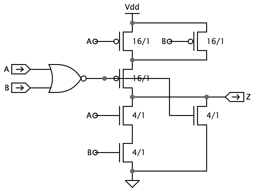
can be a challenging gate to design; here's one suggestion for how it
might be implemented based on the observation that \(\textrm{XOR}(A,B)\) is
true when \(A\) and \(B\) are not \(11\) or \(00\):
$$\textrm{XOR}(A,B) = \overline{A\cdot B + \overline{A}\cdot\overline{B}} =
\overline{A\cdot B + \overline{A + B}} = \overline{A\cdot B + \textrm{NOR}(A,B)}$$
The large, black "connection dots" in the
schematic show where crossing signal wires connect. In the figure
above, the output of the NOR2 gate connects to the gate of the PFET
then goes on to connect to the gate of the
NFET at the bottom right. It crosses over but does not connect to
the Z wire. The triangle symbol at the bottom is a connection to
ground; the T-shaped symbol at the top is a connection to \(V_{DD}\).
Click on the button below to open the Jade instance where you'll enter your design.
We've provided skeleton modules for most of the logic gates —
each module includes a schematic icon and a functional test, but
you'll need to build the schematic for any gates you use in your design.
We've provided schematics for the inverter and for the AND and OR gates,
which are built using the corresponding NAND and NOR gates.
Suggested steps:
Select the "/adder/fa" module using the module selection box at
the top. Design the circuit you'll use to implement the FA functionality
then click and drag the gates needed from the parts bin on the right into
your schematic. Arrange the gates and input/output ports tastefully,
then add wires to make the appropriate connections.
Enter a schematic for each logic gate you used in Step 1:
select
the appropriate module, then drag NFETs and PFETs from the
parts bin into the schematic to build a CMOS implementation of the
gate. You can click and drag the icons for ground and \(V_{DD}\)
from the toolbar at the top of the schematic to make connections
for the pulldowns and pullups. Remember to hook up the input/output ports.
Take a look at the /adder/inverter module to see what a finished
gate schematic looks like.
Now click the green checkmark in the toolbar in order to run
the test to verify that you've correctly implemented the gate.
Once all the necessary logic gates have been designed and
verified, return to the /adder/fa module and verify its implementation
by clicking on the green checkmark.
After your FA implementation is correct, select the /adder/adder3
module and click the green checkmark to verify correct operation of
the ADDER3 module and complete the design task.
Since this is a large circuit, the simulation will take awhile —
be patient! When this simulation completes successfully, the system
will give you credit for completing this design problem.