CMOS Technology
When entering numeric values in the answer fields, you can use integers (1000, 0x3E8, 0b1111101000), floating-point numbers (1000.0), scientific notation (1e3), engineering scale factors (1K), or numeric expressions (3*300 + 100). Useful links: Problem 1. CMOS VTC Recall from lecture that the voltage transfer characteristic (VTC) is computed by setting a gate's input voltage to a sequence of values and measuring the gate's output for each input voltage, waiting until the circuit has reached a steady state. We'll use the DC sweep capability of Jade to do the measurements and plot the results. The schematic below includes a CMOS inverter with its gate controlled by a voltage source (\(V_{GS}\)) whose value will be set to a sequence of values between 0V and 3V by the sweep tool.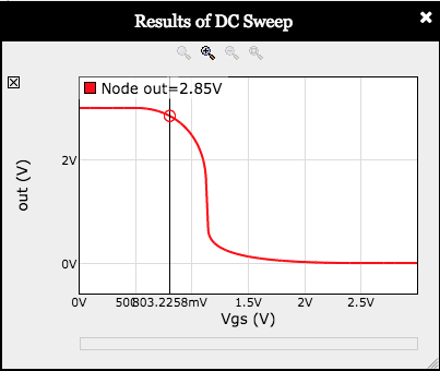 In the toolbar above the schematic, click on
to run a DC sweep and then click to accept the preset sweep
parameters. You should see a plot like the one shown on the right.
You can make the plot window bigger by dragging the thumb in the lower
right. Moving the mouse over the plot will produce a measurement for
each curve at the indicated point.
We've chosen \(V_{OL}=0.3V\) and \(V_{OH}=2.7V\).
Using the VTC (the red curve on the plot, labeled "out"),
determine appropriate values for \(V_{IL}\) and \(V_{IH}\).
In the toolbar above the schematic, click on
to run a DC sweep and then click to accept the preset sweep
parameters. You should see a plot like the one shown on the right.
You can make the plot window bigger by dragging the thumb in the lower
right. Moving the mouse over the plot will produce a measurement for
each curve at the indicated point.
We've chosen \(V_{OL}=0.3V\) and \(V_{OH}=2.7V\).
Using the VTC (the red curve on the plot, labeled "out"),
determine appropriate values for \(V_{IL}\) and \(V_{IH}\).
With all four voltage specifications in hand, please compute the low and high noise margins:
Notice that the low noise margin is much smaller than the high noise margin, compromising the noise immunity of the gate (the noise immunity is smaller of the two noise margins).
The problem is that the VTC isn't centered because in the manufacturing process we're modeling, n-channel MOSFETs have much better conductance than p-channel MOSFETs. To compensate, increase the width of the PFET beyond its initial value of 8 by double clicking the PFET in the schematic and changing the value for its scaled width. Experiment with the PFET width to find a value that approximately centers the VTC, i.e., so that the vin and vout curves intersect at \(V_{DD}/2 = 1.5V\).Determine new values for \(V_{IL}\) and \(V_{IH}\), then
recompute revised low and high noise margins:
Moral of the story: by sizing the MOSFETs so that the VTC is centered, we maximize the noise immunity of the inverter.
Problem 2. Contamination and propagation times
Let's measure the propagation and contamination times of a CMOS inverter. To provide realistic input waveforms and output loading, we'll use a chain of 3 CMOS inverters and make our measurements on the output of the middle inverter: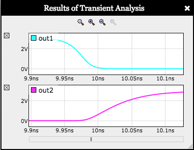 Click on
to run a device-level transient simulation, then click
to accept the preset 25ns simulation time. On the
resulting plot, zoom in on the first input transition, which should
give you a plot like the one shown to the right. To zoom in: double-click
on one of the plots (it doesn't matter which) at the time where you
want to zoom in — each double-click will increase the horizontal
magnification, but keep the plot stable at the time the mouse is
pointing to.
For these measurements, use the following voltage specifications:
$$V_{OL}=0.3V,V_{IL}=1.1V, V_{IH}=1.8V, V_{OH}=2.7V$$
We'll start by measuring the contamination and propagation times for
the falling input transition at t=10ns. The contamination time is the delay
from when the input becomes invalid as it crosses
\(V_{IH}\) and when the output becomes invalid as it
crosses \(V_{OL}\). The propagation time is the delay from when
the input becomes valid as it crosses \(V_{IL}\) and when
the output becomes valid as it crosses \(V_{OH}\).
Click on
to run a device-level transient simulation, then click
to accept the preset 25ns simulation time. On the
resulting plot, zoom in on the first input transition, which should
give you a plot like the one shown to the right. To zoom in: double-click
on one of the plots (it doesn't matter which) at the time where you
want to zoom in — each double-click will increase the horizontal
magnification, but keep the plot stable at the time the mouse is
pointing to.
For these measurements, use the following voltage specifications:
$$V_{OL}=0.3V,V_{IL}=1.1V, V_{IH}=1.8V, V_{OH}=2.7V$$
We'll start by measuring the contamination and propagation times for
the falling input transition at t=10ns. The contamination time is the delay
from when the input becomes invalid as it crosses
\(V_{IH}\) and when the output becomes invalid as it
crosses \(V_{OL}\). The propagation time is the delay from when
the input becomes valid as it crosses \(V_{IL}\) and when
the output becomes valid as it crosses \(V_{OH}\).
Now measure the contamination and propagation times for the
rising input transition at t=20ns. This time the contamination time is the delay
from when the input becomes invalid as it crosses
\(V_{IL}\) and when the output becomes invalid as it
crosses \(V_{OH}\). The propagation time is the delay from when
the input becomes valid as it crosses \(V_{IH}\) and when
the output becomes valid as it crosses \(V_{OL}\).
We now have two measurements each for the contamination and
propagation times. To arrive at the \(t_{CD}\) and \(t_{PD}\)
specifications for this inverter, choose the appropriate measurement
remembering that \(t_{CD}\) is a lower bound on the measured
contamination times and \(t_{PD}\) is an upper bound on the
measured propagation times. In real life, one would need measurements
across the range of environment conditions (e.g., power supply voltage),
input rise/fall times and possible output loadings. But, using just
the two measurements we have:
Problem 3. CMOS buffers?
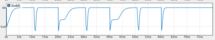
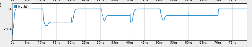
In building CMOS gates, we follow the rule of using only NFETs in the pulldown circuits and only PFETs in the pullup circuits. But why do we have that rule? Suppose we tried to build a CMOS buffer using an NFET pullup and PFET pulldown — what bad thing would happen? To find out, let's run an experiment! In the schematic below, the chain of three inverters from Question 2 have been changed to a chain of three CMOS buffers by interchanging the NFETs and PFETs.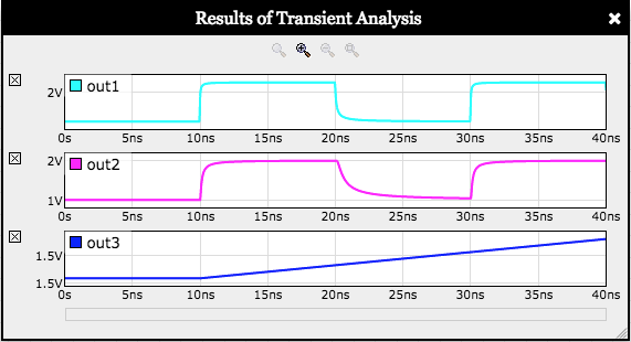
What's going on? First note that the power supply (\(V_{DD}\)) voltage is 3V and that an NFET is "off" when its \(V_{GS} = V_{G} - V_{S}\) is less than or equal to \(V_{TH}\), which is 0.5V in the manufacturing process we're modeling.
Think about the NFET pullup in the first buffer in the chain: its gate is the node in, its drain is vdd and its source is out1. The NFET pullup is "on" until its \(V_{GS}\) falls below 0.5V. When in is at 3V and the NFET's source node out1 reaches 2.5V, the NFET turns off and the source node voltage can raise no higher. So \(V_{OH}\) for the first buffer is only 2.5V, a "threshold drop" below the power supply voltage. out1 is the input node for the second buffer in the chain, hooked to gate node of the second NFET pullup. The second pullup turns off when its \(V_{GS}\) falls below 0.5, but now \(V_{G}\) is only 2.5V, so \(V_{OH}\) for out2, the output of the second buffer, is only 2.0V, two threshold drops below the power supply voltage. We're slowly losing ground here — the threshold drops are accumulating! By the time we get to the third buffer in the chain, its output is three threshold drops below the power supply voltage of 3V, so its output is unchanging at 1.5V. A similar argument applies to the "threshold raises" induced by the PFET pulldowns and the \(V_{OL}\) for each buffer increases by a threshold as we go down the chain. This is why we don't use PFETs in pulldown circuits or NFETs in pullup circuits — in that configuration we observe threshold drops in the max and min output voltages, which accumulate and cause the buffers to produce meaningless outputs.Problem 4. Design Problem: CMOS gate design
| A | B | C | F(A,B,C) |
|---|---|---|---|
| 0 | 0 | 0 | 0 |
| 0 | 0 | 1 | 1 |
| 0 | 1 | 0 | 0 |
| 0 | 1 | 1 | 1 |
| 1 | 0 | 0 | 0 |
| 1 | 0 | 1 | 1 |
| 1 | 1 | 0 | 1 |
| 1 | 1 | 1 | 1 |
Please implement \(F = C + A\cdot B\).