
Building the Beta
When entering numeric values in the answer fields, you can use integers (1000, 0x3E8, 0b1111101000), floating-point numbers (1000.0), scientific notation (1e3), engineering scale factors (1K), or numeric expressions (3*300 + 100). Useful links:- Unpipelined Beta (PDF)
- Summary of Instruction Formats (PDF)
- Standard Cell Library
- Introduction to Jade
-
Swap register contents with memory location
Usage:     MSWP (Ra, literal, Rc)
Operation: PC <- PC + 4
           EA <- Reg[Ra] + SEXT(literal)
           tmp <- Mem[EA]
           Mem[EA] <- Reg[Rc]
           Reg[Rc] <- tmp
Usage:     MVZ (Ra, Rb, Rc)
Operation: PC <- PC + 4
           if Reg[Ra] == 0 then Reg[Rc] <- Reg[Rb]
Usage:     MVZ (Ra, literal, Rc)
Operation: PC <- PC + 4
           if Reg[Ra] == 0 then Reg[Rc] <- SEXT(literal)
Usage:     LDX (Ra, Rb, Rc)
Operation: PC <- PC + 4
           Reg[Rc] <- Mem[Reg[Ra] + Reg[Rb]]
-
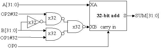
For each of the eight possible values of the three control bits
OP[2:0] indicate what operation the revised adder unit will
perform.
Usage:     LOOP(Ra, label, Rc)
Operation: literal = ((OFFSET(label) - OFFSET(current inst))/4) - 1
           PC <- PC + 4
           EA <- PC + 4*SEXT(literal)
           tmp <- Reg[Ra]
           Reg[Rc] <- Reg[Ra] - 1
           if tmp != 0 then PC <- EA
The LOOP instruction behaves like a BNE in the sense that it
branches if Reg[Ra] is not zero. But instead of saving the PC of
the following instruction in Rc, Reg[Ra]-1 is stored in Rc
instead. The destination of the branch is determined as for all
branches: the literal field of the instruction is treated as a
word offset, so it is sign-extended, multiplied by four and added
to PC+4 to produce a new value for the PC. Usually Ra and Rc
specify the same register.
Consider the following instruction sequence:loop: ADD(R1,R2,R3)
LOOP(R4,loop,R4)
...
Suppose R4 is initialized to 8 and then the two-instruction
sequence shown above is executed.
Your first step is to copy over the ALU modules you designed in Lab 3 so that we can use your ALU in the Beta. Here's what you need to do:
-
In another browser window open up the "32-bit ALU" exercise and scroll down to the
Jade window in Problem 1. In the module toolbar at the top of the
Jade window, click on
to copy your /alu modules onto the module clipboard.
Returning to this window, in the module toolbar below,
click on , which will pop
up a window to let you select which modules to copy into the "Building the Beta"
workspace. Select all the /alu modules and click "OK", which will
add the selected modules to your parts bin.
Double-check that everything's okay by editing /alu/alu
(use the Module: selection box in the module toolbar) and re-running
the tests. Hopefully the tests will pass and you're good to go!
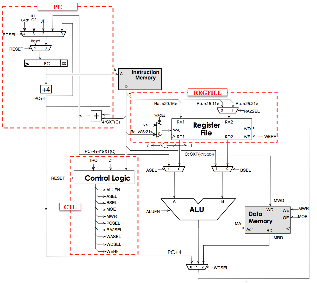
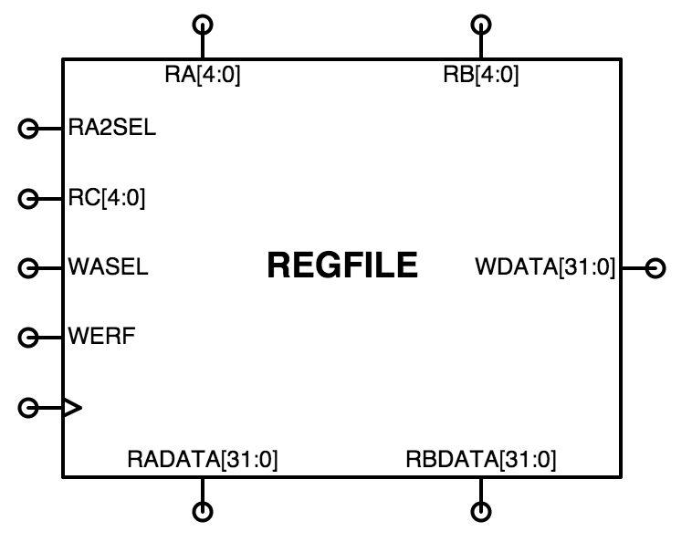 Using the module toolbar, select the /beta/regfile module to edit.
The icon for the REGFILE module is shown on the right. The
module's inputs are on the left, top, and right; its outputs are on the
bottom. The block diagram for the module's internal circuitry
is shown on the block diagram above.
The heart of the REGFILE module is a 3-port memory, built using
the MEM component (found in the toolbar above the schematic diagram).
Start your design by dragging an instance of the MEM component into
your schematic then editing its properties to set the number of ports
to 3, the width of the address to 5 (specifying 32 locations) and
the width of the data to 32. Correctly configured, the MEM component
icon should look like the one shown on the right below. Note that
the CLK inputs are labeled with the triangle symbol we
use to indicate an input triggered by a 0→1 transition.
Using the module toolbar, select the /beta/regfile module to edit.
The icon for the REGFILE module is shown on the right. The
module's inputs are on the left, top, and right; its outputs are on the
bottom. The block diagram for the module's internal circuitry
is shown on the block diagram above.
The heart of the REGFILE module is a 3-port memory, built using
the MEM component (found in the toolbar above the schematic diagram).
Start your design by dragging an instance of the MEM component into
your schematic then editing its properties to set the number of ports
to 3, the width of the address to 5 (specifying 32 locations) and
the width of the data to 32. Correctly configured, the MEM component
icon should look like the one shown on the right below. Note that
the CLK inputs are labeled with the triangle symbol we
use to indicate an input triggered by a 0→1 transition.
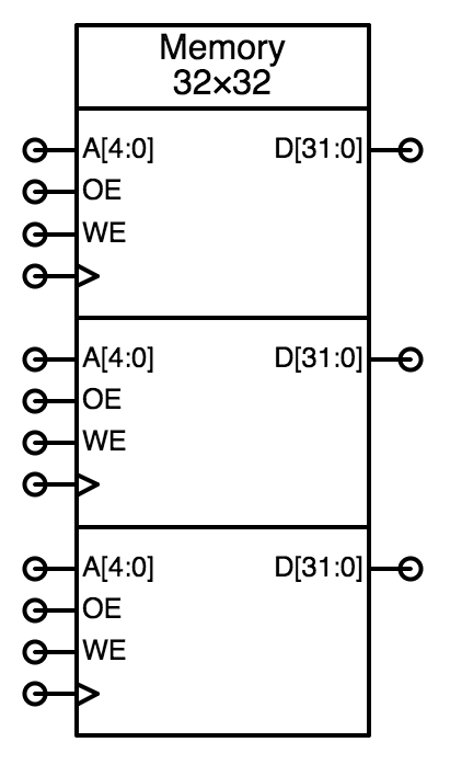 Two of the ports are used from reading values from the memory. A
read port is configured by setting the port's OE input to
1 (connect it to a wire labeled 1'1) and the WE
and CLK inputs to 0 (connect them to wires labeled 0'1).
The third port is used for writing values into the memory. A
write port is configured by setting the OE to 0 and connecting
the WE and CLK to the appropriate signals. A
write will occur on the rising edge of the CLK input if
the WE input is a 1.
Now add the RA2SEL and WASEL address muxes to the select the
addresses for the second read port and the write port. The WASEL mux
input labeled XP in the block diagram is indicating the
address of the XP register, i.e., register 30.
Two of the ports are used from reading values from the memory. A
read port is configured by setting the port's OE input to
1 (connect it to a wire labeled 1'1) and the WE
and CLK inputs to 0 (connect them to wires labeled 0'1).
The third port is used for writing values into the memory. A
write port is configured by setting the OE to 0 and connecting
the WE and CLK to the appropriate signals. A
write will occur on the rising edge of the CLK input if
the WE input is a 1.
Now add the RA2SEL and WASEL address muxes to the select the
addresses for the second read port and the write port. The WASEL mux
input labeled XP in the block diagram is indicating the
address of the XP register, i.e., register 30.
Hint: Remember that the default width of a wire is 1. The outputs
of the RA2SEL and WASEL muxes should each be 5 bits wide, the
width of a register address. So you'll need to set the widths of
the wires connecting the MUX outputs to the memory, either by giving
the wires names that implicitly specify a width, e.g., ADDR[4:0],
or by setting the wire's width property to 5.
Remember to set width of each wire if the width of the wire is
greater than 1. Jade will "transmit" the width information along
connected wire segments, so you'll only need to set the width
somewhere along the wire's run.
Note that the memory component doesn't know that location 31 of
the register file should always read as zero, so you'll have to add
additional logic around the memory that makes this happen. You can
use muxes or ANDs to force the register data for each read port to "0"
when the port address is 0b11111 (i.e., R31). Note
that the address for the second read port comes from the output
of the RA2SEL mux, so that's the value that needs to be tested for
that port.
When you're ready to test your circuit, click the green checkmark
to run the provided tests that verify your circuit has the functionality
described above. If an error is reported, look at the TEST aspect
and read the comments associated with that particular test cycle.
Now would be a good time to save your work :)
Hint: What do I do when the tests fail?
The failure notification will tell you which signal failed
verification and the simulated time at which the mismatch between the
actual value and expected occurred. The tests are actually a sequence
of 100ns testing cycles and the reported time will be at the
end of one of the cycles when the output values are checked for
correctness.
Move your mouse over the plot of the appropriate signal waveform
until the vertical time cursor is approximately at the failure time.
Then double-click to zoom in on the plots around that particular time;
zoom in enough so that all the signals for that testing cycle are
readable. Now you can figure out what the circuit was being asked to
do for that particular test and, hopefully, deduce why your circuit is
producing an incorrect output.
Control Logic (CTL)
 Using the module toolbar, select the /beta/ctl module to edit.
The icon for the PC module is shown on the right. The
module's inputs are on the left, its outputs are on the
right.
The heart of the CTL module is the control ROM, a 64-entry lookup
table addressed by the 6-bit opcode field of the instruction
OP[5:0], which outputs the appropriate values for the 18
control signals. The ROM can be constructed using MEM component
configured to have one read port and with its Contents property
initialized with the appropriate values (see the Control logic table
in the Unpipelined Beta
diagram). That diagram also has a table of ALUFN values that will be
useful when filling in the ALUFN[5:0] values for each instruction.
The contents property should be a list of 64 18-bit values. You
can use extra whitespace and the standard "//" and "/* ... */" comment
conventions to make contents more readable. "+" and "_" can be used
to separate subfields and will be ignored by the contents parser.
You can use "?" to indicate a "don't care" value for a particular digit
in a numeric value; it will be replaced by a 0 when Jade builds the
ROM contents.
To get you started, we've provided a
control ROM contents file
which you can copy-and-paste into the contents property of the MEM component.
You should then edit the control signal values specified for each of the 64
opcodes so that the ROM will generate the signals necessary for the Beta
to correctly execute instructions with that particular opcode.
Using the module toolbar, select the /beta/ctl module to edit.
The icon for the PC module is shown on the right. The
module's inputs are on the left, its outputs are on the
right.
The heart of the CTL module is the control ROM, a 64-entry lookup
table addressed by the 6-bit opcode field of the instruction
OP[5:0], which outputs the appropriate values for the 18
control signals. The ROM can be constructed using MEM component
configured to have one read port and with its Contents property
initialized with the appropriate values (see the Control logic table
in the Unpipelined Beta
diagram). That diagram also has a table of ALUFN values that will be
useful when filling in the ALUFN[5:0] values for each instruction.
The contents property should be a list of 64 18-bit values. You
can use extra whitespace and the standard "//" and "/* ... */" comment
conventions to make contents more readable. "+" and "_" can be used
to separate subfields and will be ignored by the contents parser.
You can use "?" to indicate a "don't care" value for a particular digit
in a numeric value; it will be replaced by a 0 when Jade builds the
ROM contents.
To get you started, we've provided a
control ROM contents file
which you can copy-and-paste into the contents property of the MEM component.
You should then edit the control signal values specified for each of the 64
opcodes so that the ROM will generate the signals necessary for the Beta
to correctly execute instructions with that particular opcode.
Hint: When editing a property you can enlarge the input
field by clicking and dragging on the lower right-hand corner of the
input field.
In this file the control signals have been set as if the corresponding
opcode was an illegal instruction, i.e., using the ILLOP column
of the Control logic table. The contents are formatted so that ALUFN[5]
is the most-significant bit of the 18-bit output and WERF is the
least-significant bit — see the comments in the file for the exact
order of the signals in each binary value. There's an 18-bit binary value
specifying the control signals for each of the 64 opcodes, listed in
opcode order. There's a comment at the end of each line that indicates
the opcode number and the corresponding Beta opcode, if any.
Here's a small excerpt from the middle of the file:
// alufn[5:0]
// asel, bsel
// moe, mwr
// pcsel[2:0]
// ra2sel
// wasel, wdsel[1:0], werf
0b??????_??_?0_011_?_1001  // 0b100000 ADD
0b??????_??_?0_011_?_1001  // 0b100001 SUB
0b??????_??_?0_011_?_1001  // 0b100010 MUL
0b??????_??_?0_011_?_1001  // 0b100011 DIV
0b??????_??_?0_011_?_1001  // 0b100100 CMPEQ
0b??????_??_?0_011_?_1001  // 0b100101 CMPLT
0b??????_??_?0_011_?_1001  // 0b100110 CMPLE
0b??????_??_?0_011_?_1001  // 0b100111
The first 6 bits on a line specify the values for ALUFN[5:0], the next 2 bits specify the values for ASEL and BSEL, and so on. Some of the outputs of the control ROM will have to be modified by external logic before connecting the appropriate output of the CTL module:
-
PCSEL[2:0] will have to be modified to be 1
when the current instruction is a taken branch, i.e., when
-
the instruction is BEQ and Z is 1
the instruction is BNE and Z is 0
-
MWR = 0
PCSEL[2:0] = 0b100
WASEL = 1
WDSEL[1:0] = 0b00
WERF = 1
 Using the module toolbar, select the /beta/pc module to edit.
The icon for the PC module is shown on the right. The
module's inputs are on the left, its outputs are on the
right. The block diagram for the module's internal circuitry
is shown on the block diagram above.
The heart of the PC module is the 32-bit register that holds the
current value of the program counter, which is the address in main
memory of the instruction to be executed in the current clock cycle,
PC[31:0]. The high-order bit of the register,
PC[31], is used as the supervisor bit. When the
supervisor bit is 0, the Beta is in user mode, executing programs
normally with interrupts enabled. When the supervisor bit is 1, the
Beta is in supervisor mode (sometimes called kernel mode), executing
kernel code with interrupts disabled.
The PC register can be built using the DREG component from the
parts library. You should include hardware for the bottom two bits of
the PC even though they are always 0; this will make debugging traces
easier to interpret.
The 5-input 32-bit PCSEL multiplexer selects the value to be
loaded into the PC register at next rising edge of the clock. Since
the standard cell library doesn't have any 5-input multiplexers,
you'll have to construct the logic that selects the next PC using a
combination of other components. Remember to add a way to set the PC
to 0x80000000 on reset. We'll use the RESET signal to force the PC to
0x80000000 during the first cycle of operation. We'll describe each
of the PCSEL input values in more detail below.
The PC module contains two 32-bit adders, which you can build as
ripple-carry adders using full-adder module you used in the Lab 3 in
the ARITH module of the ALU.
Using the module toolbar, select the /beta/pc module to edit.
The icon for the PC module is shown on the right. The
module's inputs are on the left, its outputs are on the
right. The block diagram for the module's internal circuitry
is shown on the block diagram above.
The heart of the PC module is the 32-bit register that holds the
current value of the program counter, which is the address in main
memory of the instruction to be executed in the current clock cycle,
PC[31:0]. The high-order bit of the register,
PC[31], is used as the supervisor bit. When the
supervisor bit is 0, the Beta is in user mode, executing programs
normally with interrupts enabled. When the supervisor bit is 1, the
Beta is in supervisor mode (sometimes called kernel mode), executing
kernel code with interrupts disabled.
The PC register can be built using the DREG component from the
parts library. You should include hardware for the bottom two bits of
the PC even though they are always 0; this will make debugging traces
easier to interpret.
The 5-input 32-bit PCSEL multiplexer selects the value to be
loaded into the PC register at next rising edge of the clock. Since
the standard cell library doesn't have any 5-input multiplexers,
you'll have to construct the logic that selects the next PC using a
combination of other components. Remember to add a way to set the PC
to 0x80000000 on reset. We'll use the RESET signal to force the PC to
0x80000000 during the first cycle of operation. We'll describe each
of the PCSEL input values in more detail below.
The PC module contains two 32-bit adders, which you can build as
ripple-carry adders using full-adder module you used in the Lab 3 in
the ARITH module of the ALU.
-
The PC+4 adder simply adds 4 to the output of the PC
register, computing the address of the instruction following the
current instruction. The output of this adder forms the
PC_INC[30:0] output of the PC module. Since we don't want
to allow a program to increment itself from user mode to supervisor
mode, we don't want to use the high-order bit of this adder's
output. Instead, ignore the high-order bit from the PC+4 adder and
use a jumper to connect PC[31] to PC_INC[31],
ensuring the supervisor bit remains unchanged when
PC_INC[31:0] is chosen as the next value of the PC.
The branch-offset adder is responsible for computing the
address of instruction specified by the literal field in
BEQ and BNE instructions. That address is
\((\textrm{PC}+4) + 4\cdot\textrm{SXT}(\textrm{ID[15:0]})\), i.e.,
multiplying the sign-extended 16-bit literal field of the
instruction by 4 to convert the word offset into a branch offset,
then adding that to the address of the next instruction. Both the
sign extension and multiply-by-4 can be done with appropriate wiring
— no gates required! The output of this adder forms the
PC_OFFSET[30:0] output of the PC module. For exactly the
same reasons given above, ignore the high-order bit from the output
of the branch-offset adder and use a jumper to connect
PC[31] to PC_OFFSET[31].
-
PCSEL=0. This input is selected during "normal" execution when the
next instruction to be executed is the one after the current instruction,
so connect this input to PC_INC[31:0].
PCSEL=1. This input is selected when a branch instruction is "taken",
i.e., the next instruction is at the address PC_OFFSET[31:0].
PCSEL=2. This input is selected during a JMP instruction, when
we use the (slightly modified) contents of the register selected by
the RA field of the instruction as the address of the next
instruction. This value is the JT[31:2] input to the PC
module. We're ignoring the low-order 2 bits of the register value
and instead should use 0b00 as the correct value for these bits
since instructions are always on a word boundary. JT[31],
the proposed new value for the supervisor bit, gets special
treatment. You'll have to add logic to compute bit 31 of this PCSEL
mux input to ensure that JMP instruction can only clear or
leave the supervisor bit unchanged. Here's a table showing the new
value of the supervisor bit after a JMP as function of
JT[31] and the current value of the supervisor bit
(PC[31]):
    current PC[31]   JT[31]   next PC[31]
    0              --         0
    1              0          0
    1              1          1
PCSEL=3. This input is selected when the current instruction has an
illegal opcode, so we want to set the next PC to 0x80000004. It's
easy to create a 32-bit-wide wire with the appropriate constant
value: simply label the wire with a name of the form number'width.
In this case we want the label 0x80000004'32.
PCSEL=4. This input is selected when the Beta is taking an interrupt,
so we want to set the next PC to 0x80000008.
When you've completed the schematic for the PC module, click on the
green checkmark in the toolbar to run the provided tests. The tests
ensure that all the functionlity described above is implemented
correctly.
Everything else
Now it's time to put it all together: using the module toolbar,
select the /beta/beta module to edit. This implementation of the Beta
subcircuit has the following terminals:
| clk | input | clock (from test circuitry): a 10MHz square wave creating a 100ns clock period. |
| reset | input | reset (from test circuitry): set by the test circuitry to 1 until after the first rising edge of clk, then set to 0 to start the Beta running. |
| irq | input | interrupt request (from test circuitry): set by the test circuitry to 1 to interrupt execution of a running user-mode program (i.e. programs where PC[31] = 0), saving PC+4 in Reg[XP], and setting the PC to 0x80000008. |
| ia[31:0] | outputs | instruction address (PC[31:0] from the PC module): address of the next instruction to be executed. This sent to the first read port of main memory. |
| id[31:0] | inputs | instruction data (from test circuitry). After the appropriate propagation delay, the main memory will drive these signals with the contents of the memory location specified by ia[31:0]. |
| ma[31:0] | outputs | memory data address (from ALU): address of data location in main memory to be read or written. This is sent to second read port of main memory. |
| mrd[31:0] | inputs | memory read data (from test circuitry): if moe is 1, the main memory will drive these signals with the contents of the memory location specified by ma[31:0]. |
| moe | output | memory read data output enable (from control logic): should be set to 1 when the Beta want to read the contents of the memory location specified by ma[31:0]. |
| mwd[31:0] | outputs | memory write data (from register file): if wr is 1, this is the data that will be written into memory location ma[31:0] at the end of the current cycle. |
| mwr | output | memory write enable (from control logic): Set to 1 when the Beta wants to store into the memory location specified by ma[31:0] at the end of the current cycle. NOTE: this signal should always have a valid logic value at the rising edge of CLK otherwise the contents of the memory will be erased. You'll need to take care in designing the logic that generates this signal — see the CTL section above for details. |
-
BSEL mux: The low-order 16 bits of the instruction need to be
sign-extended to 32 bits. Sign-extension is easy in hardware! Just
connect id[15:0] to the low-order sixteen D1 inputs
of the mux and id[15] to each of the high-order sixteen
D1 inputs.
ASEL mux and Z logic: these are
added to the RADATA[31:0] port of the register file.
When connecting the PC_OFFSET output from the PC module
to the "1" input of the ASEL mux, you should ignore the high-order
bit and use 0'1 instead, since we don't want to use the supervisor
bit as part of the LDR address.
WDSEL mux: this 3-input 32-bit multiplexer will select
the data to be written into the register file from one of three
possible sources. Sorry, no MUX3 in the parts bin, but you can use a
MUX4 and tie an input to 0'32.
IRQ logic: the Beta should only respond to an external
interrupt request when it's executing in user mode, i.e., when
PC[31] is 0. You'll need to add some logic to ensure this
functionality when generating the IRQ input to the CTL
module.

b3434c3f130d9b6ef5999d08272a66b3073e4fb19fc200f92cb344023391507ab03577cf74fa82a755bd3d2187d080cbc3ea1fe1dd37d1aac68e4bb3c41f5a86520e541410eab6d04e001e2c74fa82a755bd3d21be8da43c13845de2367ca3a45a9d177beb52e889bc1aad262636f3657c4b1f6b56b6ef897ae772b43d3e7f982a394621fdc3f92aaa3fe873948055980ddd848d57b4f5117c48966db9963b948fae862c2a52ac08aa6d7b07d53a390d2e8cba9ed8622da7fc0503cb81b78654a7f3e3f2ab64d9062b3523ddaeca0730a9c89804070df7a82ddcc3daf7ab9943d6ad008fc6304bcbc37da881b9b04e34e0a12276beab30c6a91e69bb17136e29de043d4e20e8bcf7afd89b383f5fbe922a15c88e4d025c3dc11e898a7ba3e15ab46957ff64d43afd40a5c6bd813f783e4738b828c686d0a5090ffd096e9d13523236e24994289546c0f42adfd0ae2ea9b42a4fa0895ffac6b3f804843738bdb433b9167a2613d6c436fdcbe91a9d4eaf37f43d03ce005c94bb9914c65295e5abfc3fcd53e6db999af6cd84fe05f99d4b480ca83f2a52ac08aa6d7b07d53a390d2e8cba9ede4d4d204c7166faea99bb29f200da60ef43bfb058d037a1318381920414add2bd6f487b2c886844955fbafca83f7c4808c9676bd29fc28b5d9862200c4b8a473b880c79cad8b0904865ce86030db39900f7bcbaa66de3ec44ccb64847721631fce1136a0a893fb2b17061886594b05b038dad02ea41e27b471dd545ad9d29bcc4fdf541a1366c3afce1136a0a893fb287832f72290fbaa5f0ecde4c58f17ef901cb3e9b05e2557664f1f3f03a8257b1f85b4114d165bbc28d2b07a5539a53ff30b147eeee80087984c39ae13c891676d7fbf142e2ff90e3501a91fb5a0612fc8304f537cff40622edda78f9af7b68dcade2c11aa81771233efc908b13bebef1a2a095f6e4dd077ecdb7b21e6e487ab466dd4d67b6ea2638baacf4a11d2c2394627b8b1a9c91e907272a66b3073e4fb1cb79a4253b25df83bd0dbbbe1818c97aa28e725e03db0e65affcfa58c924b8ab2c734b966bc878ab879c52f8debfef40ab64d9062b3523dd050563e3ce4b9139a28e725e03db0e65e2aa1433251ce34525597414c4802035101d027f1a8b4620156f284165d4c1a264d1d4946c04a909d381b08b566ebc836255b58980e6aeb4a0e5d7fba07b10084df02e60f6de31057cacd82643346c693ab47f9eab124bf0