
Finite State Machines
When entering numeric values in the answer fields, you can use integers (1000, 0x3E8, 0b1111101000), floating-point numbers (1000.0), scientific notation (1e3), engineering scale factors (1K), or numeric expressions (3*300 + 100).Problem 1. FSMs
A possible implementation of a finite state machine with two inputs and one output is shown below.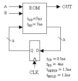
-
If the register is 5 bits wide (i.e., k = 5) what is the appropriate size
of the ROM? Give the number of locations and the number of bits in each location.
-
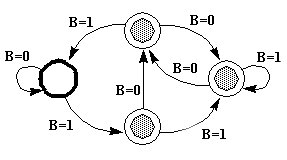
Is there a synchronizing sequence of inputs which will
return this FSM from an unknown state to its starting state?
|
|
Problem 3. Design problem: Well-formed parenthesis string checker
In 1936 Alan Turing described the "a-machine", a device that performed computations on a string of symbols according to a simple set of manipulation rules enumerated in the form of a finite-state machine (FSM). The machine consisted of- ...an unlimited memory capacity obtained in the form of an
infinite tape marked out into squares, on each of which a symbol could
be printed. At any moment there is one symbol in the machine; it is
called the scanned symbol. The machine can alter the scanned symbol
and its behavior is in part determined by that symbol, but the symbols
on the tape elsewhere do not affect the behavior of the
machine. However, the tape can be moved back and forth through the
machine, this being one of the elementary operations of the
machine. Any symbol on the tape may therefore eventually have an
innings. (Turing, 1948)
-
C++-style comment: ignore characters starting with the "//" and
continuing to the end of the current line.
-
C-style comment: ignore characters between "/*" and "*/". Note that
the ignored characters may include newlines; this type of comment can
be used to comment-out multiple lines of your file.
-
Declare one or more tape symbols. The symbol "-" (dash) is predefined
and is used to indicate that a tape cell is blank. You have to
declare symbols you use in an action statement (see below). A symbol
can be any sequence of non-whitespace characters not including "/", "\", or
the quote character. If you want to declare a symbol containing
whitespace, "/" or quote, you must enclose the symbol in quotes. You
can have more than one symbols statement in your file.
-
Declare one or more states. There are two predefined states: "*halt*"
and "*error*". The TM simulation will stop if either of these states
is reached. The "*error*" state is useful for indicating that the TM
has halted due to an unexpected condition. You can have more than one
states statement in your file. The first state specified by
the first states statement is the starting state for the TM.
-
Specify the action performed by the TM when the current state
is state and the current symbol
is symbol. First the TM will write writesymbol into
the current cell of the tape. Then the tape is moved left if "l" is
specified for the motion, right if "r" is specified and remain where
it is if "-" is specified. Finally the current state of the control
FSM is changed to newstate and the TM searches for the next applicable
action. If newstate is "*halt*" or "*error*", the TM simulation
stops. If there is no action specified for the current state and
current symbol, the TM enters the "*error*" state. Note that you have
to declare any symbols or states you use in an action
statement -- this requirement is helpful in catching typos.
-
Specifies the initial configuration of a TM tape, each tape has a
name. The various names are displayed as a set of radio buttons at
the bottom of the TM animation -- you can select which tape is loaded at
reset by clicking on one of the buttons. You can specify which cell
of the tape is to be current cell after reset by enclosing the
appropriate symbol in square brackets. For example, an initial tape
configuration called "test" consisting of three non-blank cells with
the head positioned over the middle cell is specified by
tape test 1 [2] 3If no initial head position is specified, the head is positioned over the leftmost symbol on the tape. result name symbol...
-
Specifies the expected head position and contents of the tape after
the TM has finished processing the initial tape configuration called
name. This statement is used by the checkoff system to verify that
your TM has correctly processed each of the test tapes. Whenever the
TM enters the "*halt*" state, the final tape configuration is checked
against the appropriate result statement if one has been specified and
any discrepancies will be reported in the status display at the bottom
of the TMSim window.
-
Like result except that only the current symbol is checked against the
specified value.
// 3-state busy beaver Turing Machine example

// See how many 1's we can write on a blank tape using
// only a three-state Turing Machine

states s1 s2 s3  // list of state names, first is starting state
symbols 1        // list of symbols (- is blank cell)

tape test -      // initial tape contents, blank in this case
result test 1 [1] 1 1 1 1 // expected result

// specify transistions: action state symbol state' write move
//    state = the current state of the FSM
//    symbol = the symbol read from the current cell
//    state' = state on the next cycle
//    write = symbol to be written into the current cell
//    move = tape movement ("l"=left, "r"=right, "-"=stay put)
action s1 - s2     1 r
action s1 1 s3     1 l
action s2 - s1     1 l
action s2 1 s2     1 r
action s3 - s2     1 l
action s3 1 *halt* 1 r
You'll find an instance of TMSim, our TM simulator, at the bottom
of this webpage. Here's what the TM simulator
looks like:
-
Simulator control: The five buttons are, respectively:
-
reset TM and tape to initial state;
step back to previous state and tape configuration
run the simulation for multiple steps
halt a running simulation
run the simulation for a single step
-
4 points: 2 states
3 points: 3 states
2 points: 4 states
1 point: 5 or more states
-
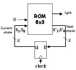
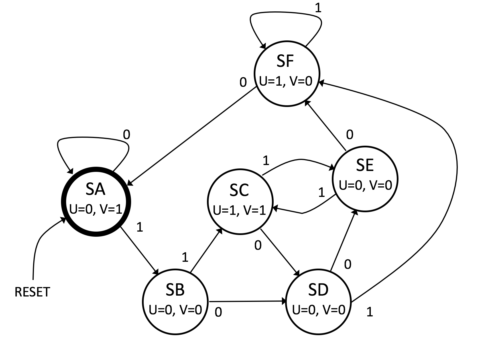
CLK. One rising clock edge the FSM should advance to
the next state which is determined from current state, the RESET
input and the IN input.
IN. A simple binary input that determined which,
along with the current state, selects which transition is chosen
from the state transition diagram.
RESET. When 1 at the rising edge of CLK, the FSM
should transition to the SA state regardless of the current state
and value of IN.
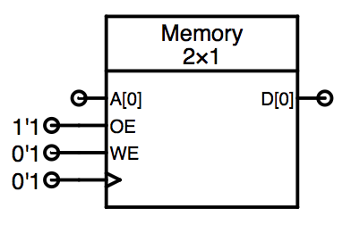
The Memory component can be used to build a read-only memory
(ROM). You can insert a memory component into your schematic by
clicking on the "MEM" icon in the schematic tab and dragging it
onto the schematic. Double-click the memory component to change
its properties. Please the see documentation for the Memory
component at the end of the
Standard Cell Library
datasheet.
To build a ROM, set the memory component to have a single
port with the desired number of address inputs and data outputs.
Connect its CLK and WE inputs to 0'1, which will disable the
ability to write into the memory, making it read-only. And
connect its OE input to 1'1 which will enable the D outputs:
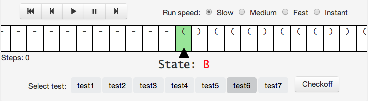
Use the Jade instance below to enter your design. To complete this
design problem, select the /fsm/fsm module and click
in the Jade toolbar and the built-in tester
will either report any discrepancies between the expected and actual
outputs, or, if your design is correct, it will record the test passed.
The tests verify that all the state transitions are correct
by checking the values of U and V while the
circuit is processing a sequence of IN values. You can
select the "Test" tab for the /fsm/fsm to see the input sequence
and the expected values of U and V at each clock
cycle. The IN is changed before the rising edge of the
clock and the values of U and V are checked just
after the rising clock edge (i.e., after the most-recent value
of IN has been processed). There are comments on each
test line indicating what the state of the FSM should be after
processing the new IN value.
// comments are allowed, don't count as content lines
// 1 line per ROM location, starting at address 0
0b0000  // binary value
5       // decimal value
0xA     // hexadecimal value
0b1_111 // binary value, _ is ignored (useful for formatting)
2fcc431e10e7913406bcc3150d997a1a4db1c6371dac28863487914e304ce5deba495c4011eef2a54679a61b2cae8c77413955e81ec58afc481f8507b00e1bbe7f0bd79eb2ea3b69eff002a7feb51151e1427c6947705710bf46f47bdb7f99fbca881869d8b249cd559dc2161163b8a792a6fd611af3a6a890100a5233ca41349038f9c26c7a2bd15c3cdcb26a88d76750ba133542a025854cef93cb23ae41da5fc371b4c3e9b54488e7a093