You can change the size of the Jade tool by clicking on
in the lower right-hand corner of the Jade window and dragging the
window to its new size.
Tool tips, etc., appear in status bar below the diagram
If Jade has been configured to allow editing of more than one
module, the module tool bar will appear at the top of the Jade window:
The module tools let you select an existing module to edit,
create a new module (),
make a copy of the current module under a new name (),
delete the current module (),
save all the user's modules to the module clipboard (),
or select previously saved modules to load from the module clipboard to the current workspace ().
Module names look like file pathnames (/x/y/z) where the hierarchy is used to display
the parts bin in organized way.
to add a component to the schematic, click on the component in the parts
bin and drag it into the schematic.
click to select a component, shift-click to add or remove a component
from the current selection. You can also click on the schematic
background, then drag out a selection rectangle which will select any component
that intersects the rectangle.
You can move selected components by clicking and dragging them to a new location.
Delete selected components by typing DEL
There's a clipboard, accessible via , , , which operate on the currently selected components.
The standard keyboard shortcuts of ctrl/cmd X, C, and V also work.
Rotate/flip selected components using , , ,
Double-click a component to edit its properties
Add wires by clicking on the open circle at component terminals or
ends of wires, drag to create a wire.
You can associate a signal name with a wire either by
connecting it to a named port component or by double-clicking the wire
and editing its name property. Wires with the same signal name are
considered electrically connected. Wires have a width, either
inferred from the signal name (e.g., "DATA[31:0]", see Extracting a
netlist below) or entered explicitly by editing the wire's Width
property. The default width of a wire is 1.
A wire can represent a multi-bit numeric constant by giving it
a name of the form number'width, where number can be
in decimal (e.g., 10), binary (0b1010), or hex (0xA); the width in bits is always
specified in decimal. For example, "5'4" would specify a wire of width
4, where the component signals are connected to gnd, vdd, gnd, vdd.
There is undo/redo support using ,
You can pan and zoom the schematic or icon diagrams using the
navigation controls in the upper left of the diagram. You can also
shift-click-and-drag on the background to pan the diagram using
the mouse.
Overview
Jade provides a framework for editing and simulating hierarchical
block diagrams. The editing and simulation tools are provided by
plug-ins, so it's easy extend the framework to support different
types of diagrams.
The basic building block is a module. Each module has one
or more aspects, which can be edited using one of the supplied
editing tools. Currently Jade has editors for the following aspects:
schematic. A circuit diagram incorporating
components (instances of other modules) with wires that run between
the component terminals. Basic components (ground, vdd, ports,
jumpers, text) are available on the toolbar; other components from
the loaded module collections are available in the parts bin. The toolbar
also has icons for the simulation tools (DC analysis, DC sweep, AC analysis,
transient analysis and module test). It's possible
to specify that the parts bin show only particular parts and the
toolbar show only a subset of the tools.
icon. When a schematic contains an instance of a module as
a component, what appears in the diagram is the module's icon, usually
a simple shape representing the component's functionality along with
terminals that allow connections to be made to the component's ports.
properties. Modules have properties (key:value pairs) that
further specify the behavior of a module, e.g., the resistor module
has a "resistance" property specifying the component's resistance.
Properties have default values, which can be overriden for each
instance of the module.
test. The test tool runs a simulation, providing a
sequence of values for module's inputs and verifying that the
expected values appear on the module's outputs. The test aspect
provides the information needed to run the test.
Extracting a netlist
To run the simulation tools on a module's schematic, Jade converts
the (possibly hierarchical) schematic into a flattened netlist that
has one entry for each primitive component listing its properties and
the signals connected to its terminals. The netlister is given a list
of primitive component modules and stops its hierachical descent when
one of these components is reached.
The extraction process has several steps:
Label each connection with its associated list of signal
names. Signal names are determined by port components or the signal
name property, if any, given to a wire. Signal names can include
lists of names and/or iterators (see below). If a wire is unnamed,
Jade will generate a name to use for the netlist.
Ensure each component in the diagram has a unique name, generating
a name for components whose name properties have not been set by the user.
Generate a netlist entry for each primitive component (instances
from the /analog collection for device-level simulation, instances from the
/gates collection for gate-level simulation). Depending on the signal lists
associated with the component's terminals, more than one netlist entry
may be generated; see below.
Recursively generate a netlist entry for each hierarchical component,
where the signal names connected to the component's terminals become the
signal names for wires connected to the corresponding ports in the
component's schematic. The component's internal signals will be prefixed
with the component's name. When the hierarchy is several levels deep,
the prefix reflects the pathname created by concatenating the names of
the components as extractor descended the hierarchy, e.g., alu.adder.cin.
Signal names should consist of letters, numbers and _, but must start
with a letter or _. For compound
signals (e.g., a bus) one can specify a comma-separated list of names
a[3],a[2],a[1],a[0]
You can use an iterator suffix of the form "[start:end]" or
"[start:end:step]" which Jade expands into the
appropriate comma-separated list. Examples:
Note that multiple suffixes are processed right-to-left.
A single component instance may generate several netlist entries. The width W
of each terminal in a component is determined from its label, e.g., a terminal
with a label of "foo" has W=1, a label of "sel[2:0]" has W=3. When the
netlist for a component is generated, each of its terminals consumes W entries
from its associated signal list. Jade will generate N components where
N = max over all terminals(length_of_terminal's_signal_list / terminal's_W)
If N*W is longer than a terminal's associated signal list, the list gets reused
in a cyclic fashion. It's a bit hard to explain in words but the results tend
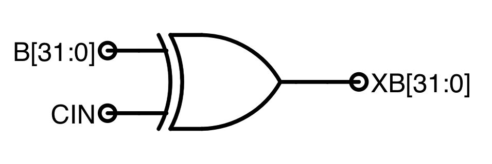
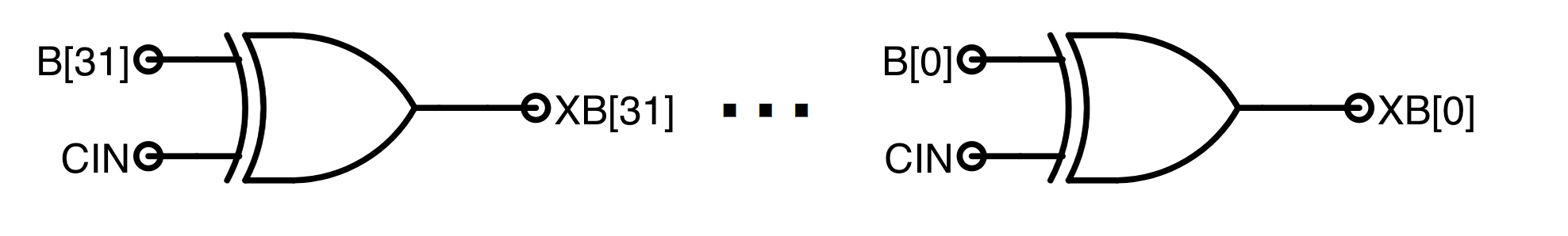
to match your expectations. For example, the following schematic using a 2-input
XOR gate
will expand into the following 32 2-input XOR gates:
Note that it is an error if (N mod W) is nonzero for any terminal.
Device-level simulation
The device-level simulation tool expects a flattened netlist containing
components from the /analog collection.
When simulating digital circuits, the easiest way to run
device-level transient simulations is to create
a test aspect specifying
.mode device
and then use the
tool to run the test. This tool will create the appropriate voltage
sources to generate the specified input waveforms, run the simulation
long enough to process all the test vectors, then examine the
simulation results to ensure the outputs have the specified values as
the specified time. The test tool will optionally plot waveforms for
the specified nodes.
One can also use primitive components to generate input waveforms
(using voltage and current sources) and examine output waveforms
(using voltage and current probes). After including the appropriate
sources and probes, the following types of circuit analysis can be
performed.
DC analysis.
Using the t=0 value for all sources, iteratively
determine the operating point of the circuit. Note that on some
circuits, the iteration may not converge on stable values for node
voltages and branch currents; you may find adding initial-voltage
components (usually on feedback nodes) will allow the analysis to
coverge. The operating voltage for each node and current through each
voltage probe will be displayed on the schematic.
DC sweep.
Perform multiple DC analyses, setting the specified sources to a sequence of values
over the range specified in the setup dialog. Useful for plotting voltage transfer
characteristics or I/V device curves.
AC analysis.
Determine the small signal response at the probed
nodes with respect to source specified in the AC setup dialog. The
response is calculated at different frequencies over the range
specified in the setup dialog. The phase (in degrees) and magnitude
(in dB) of the response is plotted as a function of log(Hz).
Transient analysis.
Determine the transient response of the circuit from
t=0 to the end time specified in the TRAN setup dialog. The resulting
waveforms are plotted as function of time for the voltage and current
probes. Note that the time to complete the simulation grows quickly
with increasing circuit size -- there's a practical limit of a few
tens of circuit nodes. The simulation proceeds by using a sequence
of linear approximations of circuit operation over a small time step.
The size of each time step is made small enough to ensure that
the error introduced by the linear approximation at that step is small.
Gate-level simulation
The gate-level simulation tool expects a flattened netlist containing
components from the /gates collection.
When simulating digital circuits, the easiest way to run gate-level
simulations is to create a test aspect
specifying
.mode gate
and then use the
tool to run the test. This tool will create the appropriate voltage
sources to generate the specified input waveforms, run the simulation
long enough to process all the test vectors, then examine the
simulation results to ensure the outputs have the specified values as
the specified time. The test tool will optionally plot waveforms for
the specified nodes.
In gate-level simulation, node values are one of the following:
0, 1 — the two binary values
X — an unknown or illegal logic value
Z — not driven, aka "high impedance"
Testing
The test aspect makes it easy to test the functionality
of a module. Here's a test for an XOR circuit with inputs A and B, and output Z:
// set up Vdd, establish signaling voltages
.power Vdd=1
// Vol, Voh set voltages generated for input signals
// Vil, Vih set voltage thresholds for determining logic values
.thresholds Vol=0 Vil=0.1 Vih=0.9 Voh=1
// test actions are applied to named groups of signals.
// A signal can appear in more than one group. Order
// of groups and signals within each group determine
// order of values on each line of test values
.group inputs A B
.group outputs Z
// set type of simulation to be performed
// device -- transient simulation; components must be from from /analog
// gate -- gate-level simulation; components must be from /gates
.mode device
/*
Tests are sequences of lines supplying test values; .cycle specifies
the sequence of actions that will be performed for each test. Available
actions are
assert group -- set values for signals in group with H,L test values
deassert group -- stop setting values for signals in group with H,L test values
sample group -- check values of signals in group with 0,1 test values
tran time -- run simulation for specified time interval
signal=val -- set signal to specified value
*/
.cycle assert inputs tran 9n sample outputs tran 1n
// the tests themselves -- one test per line
// to assert signal this cycle use 0,1; use Z or - if not to be asserted
// to sample signal this cycle use L,H; use - if not to be sampled
// whitespace can be used to improve readability, non-blank characters
// are associated, in order, with signals listed in .group above.
00 L
01 H
10 H
11 L
// (optional) produce plots showing the test inputs and/or outputs
.plot A
.plot B
.plot Z
The tests for a module can be run by clicking in the schematic toolbar.
If you'd like to see more examples, each module in the /gates
collection has a test aspect that verifies its functionality at the
device level.