Performance Measures
11. Performance Measures
Much of the attention of real-world engineers is devoted to
the exploration of alternative approaches to solving a problem
at hand, each of which involves different tradeoffs between
various cost and performance parameters.
To approach these engineering tradeoffs systematically, it is
important to have quantitative metrics of each.
Consider a digital system that performs some useful function:
perhaps it plays digitally encoded music, shows a movie on a
screen, or processes the payroll for a large corporation.
Each of these applications has some set of performance requirements:
the music player needs to generate output at some sampling
rate in real time, and the payroll program must get the checks
cut in time for payday.
How these application-level requirements translate to choice
of specific system structures and algorithms is the stuff of
engineering.
Latency versus Throughput
11.1. Latency versus Throughput
To approach such questions, we abstract requirements on the
performance of our digital components a bit.
Consider a digital building block that computes some
function, $P(x)$ for a given input value $x$.
Given several implementations of devices computing $P(x)$,
how do we compare their performance?
One obvious criterion is the answer to the simple question:
given $x$, how long does it take to compute $P(x)$?
In the case of combinational circuits, the answer is captured
in the propagation delay specification $t_{PD}$.
But we need to generalize the measure to arbitrary circuits
containing clocked components and running in the discrete time
that results from reticulating time into clock cycles.
By this metric, the device that can produce the result $P(x)$
from an input $x$ in the shortest time is clearly the performance
winner.
Depending on our application, however, this may not be the
performance parameter that interests us.
If we have a large number of independent inputs $x_1, x_2, ...$
that we need to process into results $P(x_1), P(x_2), ...$
we might care more about the
rate at which a given
device can compute $P(x)$ values from consecutive values of
$x$.
Definition:
The latency of a digital system is an upper bound on the
interval between valid inputs to that system and its production
of valid outputs.
The latency of a system is thus the time it takes to perform
a single computation, from start to finish.
The latency of a combinational device is simply its propagation
delay $t_{PD}$; for clocked devices, the latency will be a
multiple of the clock period.
Definition:
The throughput of a digital system is the rate at which
it computes outputs from new inputs.
The throughput of a system is the rate at which it accepts inputs,
or, equivalently, the rate at which it produces outputs.
Since a combinational circuit can only perform a single computation
at a time, it follows that the maximum throughput of a combinational
circuit whose latency is $L$ is simply $1/L$, corresponding to the
processing of a sequence of inputs by starting each new computation
as soon as the prior computation has finished.
The throughput measure becomes more interesting when we consider
sequential circuits which may be performing portions of several
independent computations simultaneously, a topic we visit shortly
in
Section 11.5.
Ripple-carry Binary Adder
11.2. Ripple-carry Binary Adder
Consider the problem of adding two $N$-bit binary numbers, for some
constant width $N$.
Although our focus here is on simple unsigned $N$-bit binary operands,
any adder that works for $N$-bit unsigned binary operands will also
correctly add signed $N$-bit operands represented in the
two's
complement form described in
Section 3.2.1.2,
a major attraction of the latter representation scheme.
An $N$-bit binary adder has at least $2 \cdot N$ bits of input and $N+1$ output
bits, considering the two $N$-bit operands and a single output whose maximum value
is twice the value of either operand.
For reasonable input widths -- 16, 32, or 64-bit operands are common -- a combinational
$N$-bit adder is a complex design problem.
Fortunately, we can exploit symmetries in the structure of the problem to
build viable $N$-bit adders by replicating a simple building block for each
bit position of the sum.
Single-bit Adders
11.2.1. Single-bit Adders
As a step toward adding $N$-bit binary numbers, consider the problem
of adding a
single bit of two $N$-bit binary numbers $A$ and $B$.
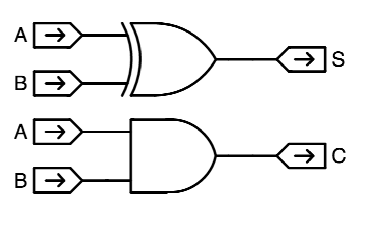
 Half Adder
We might devise a component such as the
half adder shown on the
right, whose inputs are the $i^{th}$ bits $A_i$ and $B_i$ of each operand,
and whose output is the $i^{th}$ bit of the sum $A+B$.
In defining such a module, we quickly realize that the sum $A_i + B_i$
requires two bits in its representation: the $i^{th}$ bit of the resulting
sum, as well as a potential
carry $C_{i+1}$ to the next higher-order bit
position.
This reflects the fact that the sum of the two input bits $A_i+B_i$ requires
a two-bit representation, corresponding to the two outputs of the half-adder
module.
We can implement the half adder module simply, using a 2-input XOR gate to
compute the low-order bit $(A+B)_i$ of the sum, and a 2-input AND gate to
compute the carry output $C_{i+1}$ as shown to the left.
Although a useful building block, the half-adder isn't quite
the single-bit building block we need to replicate to make an $N$-bit
adder. The half adder adds two single-bit inputs, producing a 2-bit
sum: it produces a carry output for the next higher bit position, but
lacks the additional input to accept a carry produced from an identical
module in the next lower bit position.
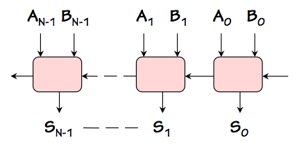
A bit of reflection convinces us that for a single-bit adder module to
be cascadeable to add $N$-bit operands, carry bits must propagate between
adjacent single-bit modules from low to high order bit positions.
We'd like a single-bit adder module that can be cascaded as shown to the right
to make an $N$-bit adder; in addition to single operand bit inputs and sum bit
output, the module needs a carry input from the lower-order bit to the right
as well as a carry output to the higher-order bit to the left.
Indeed, the requisite module must add
three single-bit inputs
($A_i$, $B_i$, and $C_{in}$) to produce the two-bit sum ($C_{out}$, $S_i$).
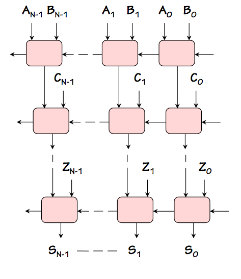
 Full Adder
The
full adder, shown to the left, is a combinational device satisfying this specification.
A ROM-based implementation of the full adder is shown in
Section 7.8.3.2.
 Full Adder Implementation
It can also be implemented using two half adders -- hence its name -- as shown to
the right.
An $N$-bit adder can be made by cascading $N$ full adders as shown above, supplying
the constant 0 as a carry into the low-order bit, and using the carry out of the
high-order bit as the high-order bit $S_N$ of the sum.
This design is called a
ripple-carry adder, owing to the need to
propagate ("ripple") the carry information from right to left along the
cascaded carry in/out chain.
In fact, this carry propagation path is the performance-limiting feature
of the ripple-carry adder.
Suppose the propagation delay specification for our full adder is $t_{FA}$.
Recall that this specification is an upper bound on the delay propagating
any valid input to a valid output.
Then the latency of our combinational $N$-bit ripple-carry adder -- its propagation
delay -- is $N \cdot t_{FA}$, reflecting a worst-case propagation path
from (say) $B_0$ to $S_{N-1}$.
If we are interested in minimizing the latency of our $N$-bit adder -- which
typically we are -- it is useful to specify the timing of our full adder in more
detail.
In particular, we might specify separate propagation delays for each input/output
path, and ask how each effects the latency of the ripple-carry adder.
If we enumerate all input/output paths through our $N$-bit adder, we find
paths that include $N$ $C_{in} \rightarrow C_{out}$ delays, but at most one
delay to a sum output bit. We conclude that, at least from this standpoint,
the $C_{in} \rightarrow C_{out}$ propagation delay is the critical specification
of our full adder implementation.
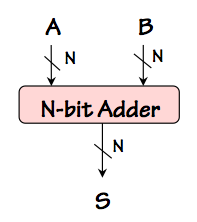 N-bit Adder
We can abstract the function performed by our N-bit adder as a building block as
diagrammed to the right: an $N$-bit adder module taking two $N$-bit binary
numbers as inputs, and producing their $N$-bit sum as a result. Variations
of this useful building block might offer an additional carry output (yielding
an $N+1$-bit sum), and a carry input; for many purposes, however, we prefer
simple adders that take and produce numbers of the same ($N$-bit) width.
Asymptotic cost/performance bounds
11.3. Asymptotic cost/performance bounds
It is often useful to characterize the behavior of cost or performance
dimensions of a design as some parameter of the design, such as the
size in bits of its inputs, becomes large.
We might, for example, characterize the latency of a 2-input ripple-carry adder
as growing in proportion to the number of bits being added.
It is useful to abstract this growth rate, which reflects the architectural
limits of the ripple-carry approach, from the actual propagation delay numbers
of a particular adder design; the latter reflects particular technology
choices as well as the architecture.
A common way to capture the abstracted growth rate of a cost or performance
specification as some parameter (say $n$) becomes large
uses one of several variations of the
order of notation
defined below:
Definition:
We say $g(n) = \Theta(f(n))$, or
"$g(n)$ is of order $f(n)$",
if there exist constants $C_2 \geq C_1 \gt 0$
such that for all but
finitely many integral $n \geq 0$,
$$C_1 \cdot f(n) \leq g(n) \leq C_2 \cdot f(n)$$
We use the notation $g(n) = O(f(n))$ to specify that $f(n)$ satisfies the
second of these inequalities for some $C_2$, but not necessarily
the first.
The $\theta(...)$ notation specifies both upper and lower bounds
on the growth it describes, while the weaker $O(...)$ constraint specifies
only an upper bound.
Thus the $O(...)$ notation is useful primarily for specifying upper bounds on
costs (such as the time or space taken by an algorithm), and is commonly
used in such contexts.
The $\theta(...)$ is useful for specifying tight bounds on both costs
(which we'd like to minimize) and performance parameters like throughput
(which we'd like to maximize).
Note that the constant factors $C_1$ and $C_2$ in these definitions
allow multiplicative constants to be ignored, while the
finitely
many exceptions clause effectively ignores additive constants
in the growth characterization.
One is left with a formula that captures the algorithmic form of the
growth as a function of the parameter -- for example, whether it is linear, quadratic,
polynomial, or exponential -- while
ignoring complicating detail.
Some examples:
- $n^2+2\cdot n+3$ = $\theta(n^2)$, since
$$n^2 \le n^2+2\cdot n+3 \le 2\cdot n^2$$ "almost always"
(i.e., with finitely many exceptions);
- $log_2(n+7) = \theta(log(n)) = log_{10}(n+88)$,
since the base of the logarithm and the added constants amount to constant factors;
- ${37589 ^ {34 \cdot 577} \over {\sqrt 17}} = \theta(1)$, as its value is constant
(usually described as $\theta(1)$ or $O(1)$);
- $n^2 = O(n^3)$, but not $\theta(n^3)$, as the asymptotic growth
of $n^3$ is an upper bound on that of $n^2$ but not a lower bound.
Asymptotic latency of N-bit Ripple Carry Adders
11.4. Asymptotic latency of N-bit Ripple Carry Adders
Returning to our N-bit ripple-carry adder, we quickly recognize that its asymptotic
latency is $\theta (N)$ owing to the worst-case propagation path along the carry
chain from low to high-order full adder modules.
We have noted that the constant of proportionality is dictated by the propagation delay
to the carry output of the full adder;
minimization of this delay will improve the performance of the adder, but only by
a constant factor.
Improving the asymptotic performance, say to $\theta (log N)$, requires a more serious
improvement to the architecture of the adder.
We will explore such improvements shortly.
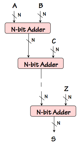
Before doing so, however, it is instructive to generalize our N-bit ripple carry adder
to more than two operands.
Given the $\theta(N)$ latency of our $N$-bit ripple-carry adder, it might seem sensible
to add a large number $M$ of $N$-bit operands using a tree of $N$-bit adders, much like
the tree of gates described in
Section 7.7.2.
If the latency of a two-operand $N$-bit full adder is $O(N)$, we could reason
that a
tree of such adders of depth $d$ would add $M = 2^d$ $N$-bit operands in $O(d \cdot N)$
time, yielding a latency of $O(N \cdot log M)$ bound for our $M$ operand by $N$ bit adder.
This reasoning, however, uses only the worst-case latency characterization of our $N$-bit ripple
carry adder and ignores the fact that some of its input-output paths are faster; a more detailed
analysis yields a less pessimistic bound on the latency of our $NxM$ ripple-carry adder.
Consider a simple cascade of $N$ bit adders to compute $S = A+(B+(C ... +Z) ... )$ for some
number of $N$-bit operands $A, ... Z$, as shown on the left.
Again, given a cascade of $M$ $N$-bit adders each having a $O(N)$ latency, we might expect
the latency of an $M$-operand adder constructed this way to exhibit $O(N \cdot M)$ latency.
While $O(N \cdot M)$ is a valid upper bound, a closer look reveals that there is no actual
input-output path through this circuit whose cumulative propagation delay grows as $O(N \cdot M)$.
This suggests that a more detailed analysis might lead to a tighter bound on the latency of
the circuit.
 NxM Ripple Carry Adder
To see this, we can expand the adder cascade into a two-dimensional array of full adders
as shown to the right, each row adding a new operand to the accumulated sum
coming from the row above.
Note that signals propagate through this array in only two directions:
the carry signals propagate from right to left, while the sum signals propagate
from top to bottom. There is no case where a signal propagates to the right
or upward.
While there are many input-output paths to be considered, each is made up of
segments propagating to the left or downward.
We conclude, from this observation, that the worst-case input-output propagation
delay grows in proportion to the sum of the width and height of the array.
Since the width grows in proportion to $N$ and the height in proportion to $M$,
we conclude that the longest propagation path -- the critical path that bounds
the latency -- grows as $O(N + M)$ rather than $O(N \cdot M)$.
Since we can actually demonstrate a path whose cumulative propagation grows
as $N+M$, this bound is tight; thus we are entitled to characterize the latency
of this adder as $\theta(N+M)$, using $\theta$ rather than $O$ to indicate
both upper and lower bounds on the latency.
Pipelined Circuits
11.5. Pipelined Circuits
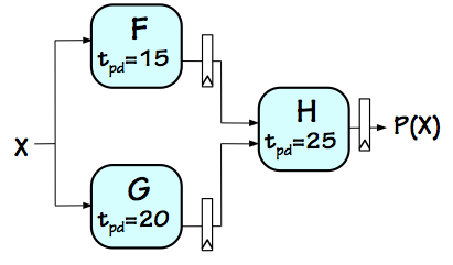
Consider a combinational circuit to compute some function $P(X) = H(F(X), G(X))$
given the value of the input $X$.
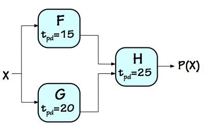 Combinational P(X)
Assuming we have combinational modules that compute the component functions $F$, $G$, and $H$
with propagation delays of $15ns$, $20ns$, and $25ns$ respectively,
the straightforward circuit on the left computes $P(X)$ with a latency of
$45ns$. Note that for this discussion the time unit is arbitrary so long as it is used consistently.
Since the combinational circuit can perform only a single $P(X)$ computation at a time,
its throughput is simply the reciprocal of its latency $1/45ns$, or about $22.22$ MHz.
This is simply the rate at which we can perform computations on our combinational
device by presenting one input after another at the maximal frequency.
If we have a large number $N$ of inputs $X_1, X_2, ... X_N$ for which we need to compute
$P(X_1), P(X_2), ... P(X_N)$, we are likely to be more interested in throughput than
in latency, as the total time for $N$ computations will be on the order of $L + N / T$ for
throughput $T$ and latency $L$.
One observation we might make about our combinational circuit is that each of
its components spends much of the $45ns$ propagation delay idle.
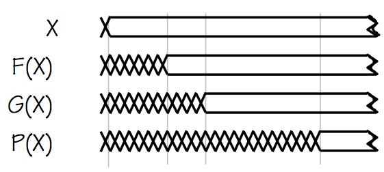 P(X) Signal Timing
From the signal timing diagram on the left, we observe that the computation of
$P(X)$ breaks down into two phases: during the first $20ns$ after a new value of
$X$ is supplied, the $H$ component is waiting while $F(X)$ and $G(X)$ are
busy computing their output values. During this phase, $H$ has invalid inputs
and can do no useful computation. Once $F(X)$ and $G(X)$ are have become valid,
a second phase is entered in which
$H$ computes the output $P(X)$ while the $F$ and $G$ modules perform no useful
computation other than maintaining valid inputs to $H$.
This observation reveals that we are not fully utilizing the computational
resources of the circuit's components: each component performs useful work,
in the sense of computing new values from a newly-supplied input, during only one
of these two phases of the computation.
We might be tempted to supply a new input $X_{i+1}$ during the second phase
of the computation of $P(X_i)$, getting the jump on a new computation by
the $F$ and $G$ modules while $H$ is completing the previous computation.
However, a new input $X_{i+1}$ will contaminate the outputs $F(X_i)$ and $G(X_i)$
that are being used by $H$, which depends on valid inputs for the duration of
the second phase. In order to guarantee a valid $P(X_i)$ value, we need to
maintain valid, stable values at the inputs of $H$ during its entire propagation
delay.
However, we can use relatively cheap
registers to maintain stable
values rather than combinational logic with stable inputs.
 Pipelined P(X)
If we divide our combinational circuit into two
pipeline stages
corresponding to the two phases of the computation, and put registers on
all outputs of each stage as shown to the right, the result is a 2-stage
pipelined circuit which performs the same computation as our
combinational circuit.
Following our single-clock synchronous discipline, all registers share a
common periodic clock input.
If we choose an appropriately long clock period, an input $X_i$ presented
at the input near the start of clock cycle $i$ will cause the values
$F(X_i)$ and $G(X_i)$ to be loaded into the registers at the outputs of the
$F$ and $G$ modules at the start of clock cycle $i+1$, where they remain
until the start of clock cycle $i+2$ when the value $P(X_i)$ is loaded
into the register at the output of $H$.
If the timing parameters of the registers is negligible compared to
the delay of other modules, we can do an approximate analysis assuming
"ideal" (zero-delay) registers. Our first observation is that the minimum
clock period that can be used for this pipelined circuit must be long
enough to accommodate the longest combinational path in the circuit:
in this case, the two paths through the $25ns$ $H$ module.
Thus the fastest we can clock this circuit is a clock period of $25ns$,
or a clock frequency of $40$ MHz.
Since it takes
two clock cycles to perform the computation of
$P(X_i)$, the latency of our pipelined circuit is now $50ns$, somewhat
longer than the $45ns$ latency of the original combinational circuit.
However, this pipelined circuit has the virtue that we can begin a
new computation by supplying a new input on
every clock
cycle.
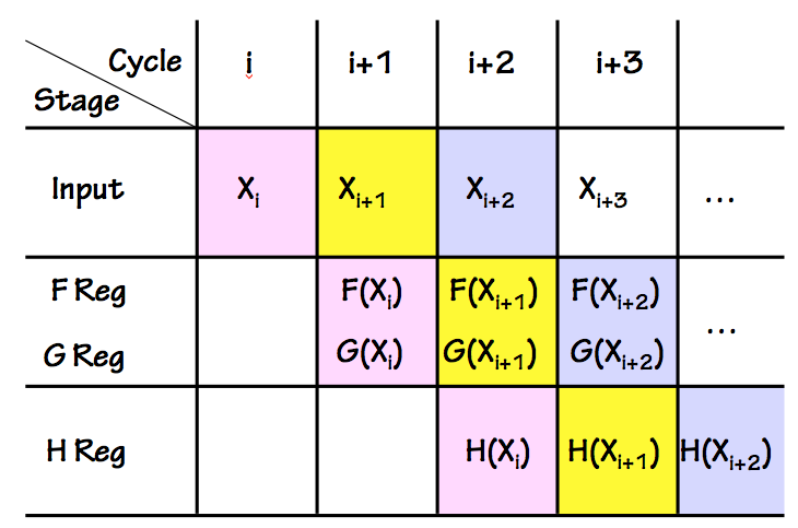 Pipelined P(X) Timing
Since the computation of each $P(X_i)$ value takes two clock cycles,
during each cycle each stage of the pipeline can be working on a
different stage of an independent computation. The timing of consecutive
computations is often summarized in a
pipeline timing diagram
like the one on the right, showing consecutive clock cycles on the horizontal
axis and successive pipeline stages on the vertical axis. Note that at
each active clock edge (vertical lines in the diagram) each $X_i$ computation
moves to the next pipeline stage, progressing diagonally down through the
diagram.
If we keep our pipeline full by supplying a new $X_i$ at each $i^{th}$ clock cycle
(and reading the corresponding $P(X_i)$ at clock cycle $i+2$), the rate at
which we are performing computations -- the throughput of our pipeline --
is just the clock frequency of $40$ MHz (the reciprocal of our $25ns$ clock
period).
Thus adding registers to convert our combinational circuit to a clocked
pipelined version degraded the latency but improved the throughput, a tradeoff
typical of pipelined circuits.
Any combinational circuit can be converted into a pipelined circuit
performing the same computation by adding registers at carefully
selected points.
The addition of the registers actually
lengthens input-output paths,
so it actually
increases latency; however, judicious selection of
register locations can improve throughput significantly.
The magic by which pipelining improves throughput involves
(a) enabling a form of
parallel computation by allowing the
pipelined circuit to work on several independent computations simultaneously;
(b) utilizing circuit components for a larger fraction of the time; and
(c) breaking long combinational paths, allowing a high clock frequency.
Well-formed Pipelines
11.5.1. Well-formed Pipelines
Simply adding registers at arbitrary locations within a combinational
circuit does not generally increase throughput; in fact, indiscriminant
insertion of registers will likely change the computation performed
by the circuit in undesirable ways.
 Ill-formed pipeline
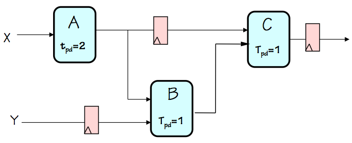
Consider, for example, the circuit on the left, a failed attempt at pipelining
a combinational circuit made using combinational components $A$, $B$, and $C$.
It was created from a working combinational circuit that computed, for each $X_i, Y_i$
input pair, an output value $C(A(X_i),B(Y_i, A(X_i)))$ by adding three registers.
The added registers, however, delay the progression of input values by varying
numbers of clock cycles as they propagate through the circuit. Imagine a
sequence of input pairs $(X_1, Y_1), (X_2, Y_2), ...$ being applied to the
$X$ and $Y$ input terminals on successive clock cycles, in an attempt to
perform the computation on a succession of independent inputs.
From the diagram, we see that the inputs to the $B$ module on a given clock
cycle will be the values $A(X_i)$ and $Y_{i-1}$; the $B$ module will compute
some confused value by mixing inputs from supposedly independent computations!
We conclude that the circuit is not pipelined in the sense of our earlier, happier
example; it does not perform the same computation as its orignal combinational
version, inproving throughput by overlapping different phases of successive
computations.
The problem illustrated by this ill-formed pipeline is that it fails to cleanly
separate values associated with one set of inputs from those of another:
values from successive computations interfere with each other as they progress
through the circuit.
Happily, a simple discipline allows us to avoid this problem:
a necessary and sufficient condition for a
well-formed pipeline
is that it have an identical number of registers on each input-output path.
By this standard, our failed example is not a well-formed pipeline.
We formalize this fact in the following definition:
Definition:
A K-Stage Pipeline
("$K$-pipeline", for short)
is an acyclic circuit having exactly $K$ registers on every
path from an input to an output.
Note that by this definition, a combinational circuit
is a $0$-pipeline.
It is useful to view a $K$-stage pipeline for $K>0$ as $K$ cascaded
pipeline stages, each consisting of combinational
logic with a single register on each output.
This view leads to our convention that
every pipelined circuit ($K$-pipeline for $K>0$) has one or
more registers on every
output. Such a convention is
useful for a number of reasons; it allows, for example,
a $k$-pipeline and a $j$-pipeline to be cascaded to create a
$(k+j)$-pipeline.
For our synchronous pipelines (adhering to the single-clock synchronous
discipline), the period $t_{CLK}$ of the shared clock must be sufficient to cover
the longest combinational delay (plus register propagation and setup
times). In this case,
- the latency of the $K$-pipeline is $K \cdot t_{CLK}$;
-
the throughput of the $K$-pipeline is the
frequency of the shared clock, or $1 / t_{CLK}$;
and
-
Inputs for the $i^{th}$ computation are presented during clock
cycle $i$, and corresponding outputs are available during clock
cycle $i+K$.
These rules characterize the externally-observable behavior of a
$K$-stage pipeline: it takes a new input each clock cycle, and
returns the corresponding output $K$ cycles later.
This implies that the circuit maintains internally the state of $K$
simulaneous but independent computations: at every instant, it
has $K$ latent outputs represented within its $K$ pipeline stages.
Pipeline Methodology
11.6. Pipeline Methodology
Given the constraint that a well-formed pipeline has the same
number of registers on every input-output path, it is useful
to develop a systematic method to convert an arbitrary combinational
circuit to a well-formed pipeline offering improved throughput.
While there are many possible approaches to this task, we sketch here
an intuitive, informal technique that serves simple pipelining
problems well.
 Combinational Version
Our problem is to start with a combinational circuit, such as that
shown on the left, and convert it to a $K$-pipeline that performs
the same computation by inserting registers at appropriate points.
The choice of "appropriate points" for the registers raises two
separable issues: (a) ensuring that the result is indeed a well-formed
$K$-pipeline for some value of $K$; and (b) ensuring that the pipelined
circuit actually offers better throughput than the original combinational
version.
We deal with these two issues in the following sections.
Ensuring well-formedness
11.6.1. Ensuring well-formedness
Note that each component of the combinational example is marked
with its propagation delay, and that the diagram is laid out so
that all signal propagation is left-to-right. While the latter
constraint is not essential to our technique, it makes the
pipelining task easier and less error-prone.
 3-Stage Pipelined Version
Our basic approach is to annotate our combinational circuit
by drawing contours through it that identify boundaries between
pipeline stages, as shown in red on the diagram to the right.
Each red contour slices through a set of signal lines in the
diagram, and thereby partitions the combinational circuit
such that its inputs are all on one side of the contour and
its outputs are on the other.
It is important that the data on the signal lines all cross the
contour in the same direction.
Each contour we draw identifies the
output edge of
a pipeline stage; thus, the first contour we establish is
one that intersects all outputs of the combinational circuit.
Subsequent contours are strategically chosen to break long
combinational paths, improving throughput.
We then make a pipelined version of our combinational circuit by
inserting a register at every point where a signal line
crosses a pipeline contour.
Every input-output path thus crosses each contour exactly
once; given $K$ contours, the result is necessarily a
well-formed $K$-pipeline.
Notice that, with our choice of pipeline boundaries leading to
the 3-stage pipeline shown,
the longest combinational path (and consequently shortest clock period)
is $8ns$. Given $3$ stages at an $8ns$ clock period,
our pipeline has a latency of $3 \cdot 8ns = 24ns$ and a throughput
of $1 / 8ns = 125 MHz$.
To summarize our technique for generating a $K$-stage pipeline from
a combinational circuit:
- Draw a first pipeline contour that intersects every
output of the combinational circuit.
This provides a template for implementation of a $1$-stage
pipeline, usually an uninteresting implementation choice.
- Draw additional contours determining boundaries between
pipeline stages. Each contour must (a) partition the circuit
by intersecting signal lines, and (b) intersect lines so that
every signal crosses the contour in the same direction.
Each additional contour increases the number of pipeline stages
by one.
- Implement the pipelined circuit by inserting a register at
every point in the combinational circuit where a signal line
crosses a pipeline contour.
- Choose a minimal clock period $t_{CLK}$ (equivalently, a maximal
clock frequency) sufficent to cover the longest combinational
path within the circuit.
Unless ideal registers are assumed, such paths must include
the propagation delay of source registers as well as setup
times of destination registers.
- The result is a $K$-stage pipeline (where $K$ is the number of
contours) whose throughput is $1 / t_{CLK}$ and whose latency is
$K \cdot t_{CLK}$.
Optimizing Throughput
11.6.2. Optimizing Throughput
Not every well-formed pipeline offers a performance improvement over
its combinational counterpart, or over alternative pipelines with
fewer stages (and hence less hardware and performance cost).
In general, it is worth adding a pipeline stage only when that
stage reduces the critical (longest delay) combinational path,
and consequently allows a faster clock and correspondingly higher
throughput.
To illustrate, consider the simple 3-component combinational circuit
diagrammed to the left.
Again, the latency (propagation delay) of each component is marked.
We notice that the latency of the circuit, dictated by the cumulative
propagation delay along its longest input-output path, is $4$,
with a consquent throughput of $1/4$.
It is instructive to look at this circuit, and propose how it might
be pipelined to maximize its throughput.
For this simple example, we will suffer the tedium of exploring
reasonable possibilities exhaustively, assuming ideal (zero delay)
registers.
Since our convention requires registers on each output of any
pipelined circuit, the first pipeline stage boundary we draw
intersects each output of the combinational circuit as shown to the right.
The resulting circuit (after adding registers at intersections of our
red contour with signal lines) is a well-formed 1-stage pipeline.
Although this is a valid pipelined circuit, since registers are
added only at its outputs, no combinational paths are shortened.
Since the longest combinational path still encounters a propagation
delay of $4$, $4$ is the shortest clock period that can be used
with our 1-stage pipelined version, yielding a latency of $4 \cdot 1 = 4$
and a throughput of $1 / 4$ assuming ideal registers. Our single-stage
pipelining gained no performance, and cost us some hardware (for the
registers).
If we assumed real (rather than ideal) registers, the added register
propagation delays and setup times would slow the clock a bit further,
actually lowering performance relative to the combinational circuit.
The opportunity for real performance enhancement comes when we add a
second pipeline stage, as indicated by the second contour in the diagram
to the left.
Here we have noticed that the $A$ component has twice the delay of the
$B$ and $C$ components, and have chosen a pipeline stage boundary
which isolates the slow $A$ from the faster components.
Assuming ideal registers, the longest combinational delay in this
$2$-stage pipeline is $2$, allowing a clock period as short as $2$
time units. This yields a latency of $2 \cdot 2 = 4$ and a throughput
of $1/2$, doubling the rate at which the circuit can perform independent
computations.
Encouraged by the performance improvement gained by our $2$-stage pipeline,
we might expect additional stages to further improve throughput.
To the left we show a contour adding a third pipeline stage, defining
a valid $3$-stage pipelined version of our original combinational circuit.
However, we note that the longest combinational path within this circuit
remains $2$, so the clock period remains $2$ and the throughput $1/2$
like that of the $2$-stage pipelined version. However, the third stage
increases the latency to $2 \cdot 3 = 6$, degrading the performance from
the cheaper $2-$stage version.

The performance characteristics of the four versions of our circuit are
summarized in the table to the left.
It is worth observing that since the clock period (and hence the throughput) of
any pipeline is limited by the longest combinational delay in the circuit,
it is limited by the propagation delay of the slowest combinational
component in that circuit.
If the slowest components are isolated in separate pipeline stages
and the clock period chosen to barely cover the propagation delays
of these bottleneck components, there is no performance advantage
to adding further pipeline stages.
Hierarchical Pipelines
11.7. Hierarchical Pipelines
The slowest-component bottleneck illustrated in the previous
section can be mitigated by replacing slow combinational components
with pipelined equivalents.
Suppose, in the example of the previous section, it were possible to replace
the combinational $A$ component whose latency of $2$ constrains the clock
period with a $2$-staged pipelined $A'$ module capable of operating at
a clock period of $1$.
The resulting circuit could operate as a $4$-stage pipeline, sustaining
a clock period of $1$, a throughput of $1/1$ and a latency of $4 \cdot 1$
as shown on the right.
Note that we have drawn two pipeline contours
through the
$2$-stage pipelined $A'$ module, reflecting the two registers it
includes on each input-output path.
In general, it is straightforward to incorporate pipelined components
into pipelined systems.
Given a pipelined system whose performance is limited by the propagation
of a specific combinational component, pipelining that bottleneck component
is often the preferred solution.
Component Interleaving
11.7.1. Component Interleaving
It is not always practical to pipeline a bottleneck combinational
component in a design, either for technical or practical reasons
relating, for example, to the inaccessibility of the internals of
a critical component.
The bottleneck $A$ module of the prior example might be a black box
library module whose supplier offers no pipelined equivalent nor
grants engineering access to its implementation details. Such a
constraint would seem to restrict us to a clock period of 2 and
correspondingly low throughput of our system.
Fortunately, there are alternative strategies to get around this
performance bottleneck.
We begin by the simple observation that if one instance of some
component $X$ offers throughput $T_X$, we can use $N$ instances
of $X$ running in parallel to achieve an aggregate throughput
of $N \cdot T_X$.
We may need some surrounding logic to route inputs to and outputs
from our farm of parallel $X$ modules, but clearly the throughput
of any module can be scaled up by simple replication.
Armed with this insight, we might ask how to double the throughput
of the bottleneck $A$ module in our example by using
two
$A$ modules rather than a single one.
It would be convenient, for example, if we could use two $A$ modules
to build a plug-in replacement for $A$ whose external behavior
is precisely that of a 2-stage pipelined $A$ module. Such a
replacement could simply be used as a component in the 4-stage
pipelined approach shown above.
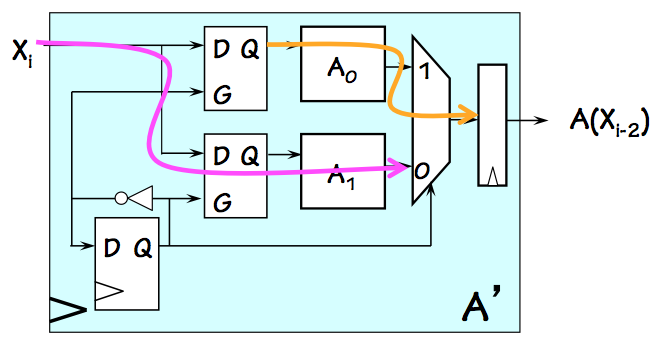 2-way Interleaved Module
One approach to building pseudo-pipelined components involves
interleaving
the execution of replicated instances of that module, using circuitry like that
shown at the right.
This circuit uses two instances of the $A$ module, labeled $A_0$ and $A_1$,
each with a propagation delay of $2$ to emulate a $2$-stage pipelined $A'$ module
that can be clocked with period 1.
Note that the flip flop in the lower left corner flips value on each
active clock edge, distinguishing between even and odd cycles.
The two latches connected to the $X_i$ input latch input data on even
and odd cycles, respectively, and hold the data as stable output for
the nearly two clock cycles it takes their $A$ module to compute a
valid result.
During an odd clock cycle, $Q=1$ and the current $X_i$ input is routed through
the lower latch and $A_1$, stopping at the output mux (purple arrow);
meanwhile the $X_{i-1}$ input latched during the previous clock cycle remains in the
upper latch, where it propagates through $A_0$ and the output mux (yellow arrow)
to be loaded into the output register at the next active clock edge.
The roles of the latches alternate every cycle, giving each $A$ component
the required two cycles to complete its computation.
Consistent with the specifications of a two-stage pipeline, however, the
2-way interleaved module takes a new input on every clock cycle and produces
the corresponding output two cycles later.
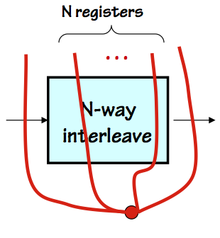 N-way Interleaving
The interleaving technique can be generalized to emulate the behavior of
an $N$-stage pipeline by replicating $N$ copies of a combinational module.
An $N$-way interleaved module can be incorporated into a pipelined
hierarchy by allowing $N$ pipeline contours to intersect the interleaved
module, implying the presence of $N$ registers on each input-output path
through that module.
While that implication may not be literally valid (as our 2-stage interleaved
module illustrates), its critical behavioral characteristic is preserved:
an $N$-clock delay between presenting inputs and appearance of corresponding
outputs.
Pipeline Issues
11.7.2. Pipeline Issues
Any combinational circuit can be partitioned into well-formed pipeline
stages, with potential gains in throughput.
Since the throughput of a pipelined circuit is constrained by
its clock frequency, we generally maximize throughput by minimizing
the longest combinational path within any pipeline stage.
The clock period chosen for such a pipeline must be sufficient to
cover this propagation delay plus the propagation delay and setup time
of the registers used for the pipelining.
As we increase the number of pipeline stages to improve throughput,
the cost and delay of the pipeline registers themselves may dominate
other design parameters.
Consider a complex combinational circuit constructed entirely from
2-input NAND gates having a $t_{PD}$ of 10ps.
Pipelining this circuit for maximal throughput would place at least
one pipeline stage boundary between
every pair of connected
gates, allowing the resulting circuit to be clocked with a period of
10ps plus the register $t_{PD}$ and setup times.
If these were 35ps and 5ps, respectively, the minimum clock period
would be 50ps, for a throughput of 20 GHz.
This design would be very costly, owing to the number of flip flops
required.
Allowing for a 2-gate delay in each stage would cut the number of
stages in half, yet allow a 60ps clock cycle for a marginally lower
throughput at dramatically reduced cost.
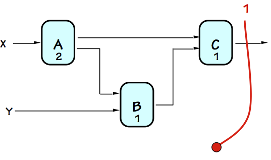
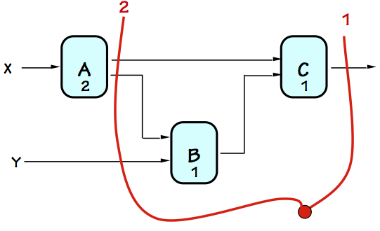
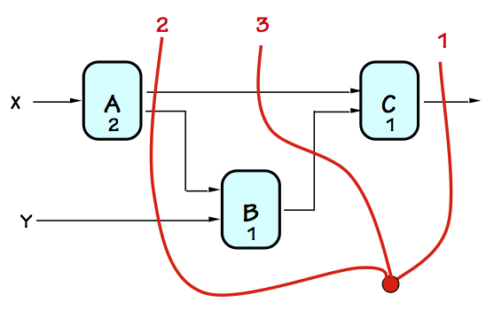
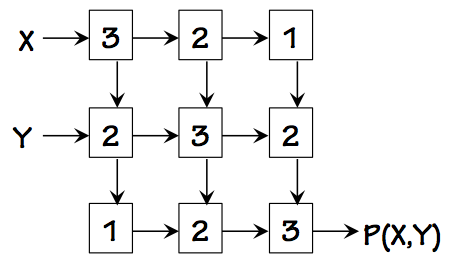 Combinational P(X,Y)
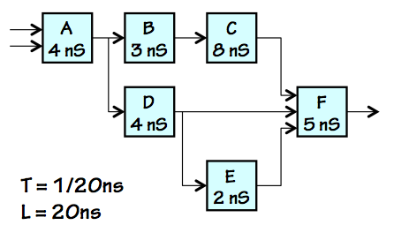
Consider a 9-component combinational circuit to compute some function $P(X,Y)$
from $X$ and $Y$ inputs, shown in the diagram to the left.
Each block is a (different) combinational component, and is marked with its
propagation delay.
Arrows on the interconnections indicate the direction of signal flow; the diagram
is drawn so that signals flow generally down and to the right.
If we were asked to pipeline this circuit for maximum throughput, we might
begin by determining what the target throughput might be.
Since the slowest components in the diagram have a propagation delay of 3,
we recognize that pipeline boundaries within this circuit will not allow a
clock period below 3, even using ideal (zero-delay) registers; so our
goal becomes drawing pipeline boundaries such that the worst-case
combinational path has a cumulative delay of 3.
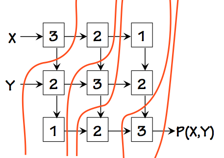
One way to do so is shown to the right.
Note that, per our convention, one pipeline boundary goes through each output
of the circuit (of which there is only one in this case, marked $P(X,Y)$).
Each of the slow components marked 3 is isolated in a pipeline stage, although
there are several stages that have paths through two components whose total
propagation delay is 3.
A total of five stages is necessary to get the clock period down to 3.
Note that our well-formed pipeline construction requires a register on
the $Y$ input but none on $X$. It also places back-to-back registers,
with no intervening logic, on several wires. While this may seem wasteful
such patterns are commonly required to assure that every input-output path
has the same number of registers.
Alternative Timing Disciplines
11.8. Alternative Timing Disciplines
As we combine sequential (clocked) components to make bigger
sequential systems, we need an engineering discipline to control
the timing of operations by each component, and to integrate their
effects into a coherent system behavior.
While our examples will focus on simple, widely used approaches,
it is worth noting that there are reasonable alternatives
whose usefulness and popularity vary among application arenas,
engineering cohorts, and chapters of the history of digital
systems engineering.
In this section, we briefly sketch the universe of timing disciplines
and several interesting variants on our simple synchronous approaches.
Synchrony vs. Localization
11.8.1. Synchrony vs. Localization
In our taxonomy of control disciplines, we distinguish between two
separable engineering choices:
-
synchronous versus asynchronous systems,
the distinction being whether signal changes are synchronized
with respect to a common clock (synchronous) or may happen at
arbitrary times (asynchronous).
-
globally versus locally (or self) timed systems,
an architectural choice between centralized logic for controlling
the timing of component operations and distributing the logic
among the components themselves.
These two choices divide the universe of timing disciplines roughly into
four quadrants, of which three have serious followings among the engineering
community and are discussed in subsequent sections.
The fourth,
Asynchronous Globally-timed Systems, involves centralized
generation and distribution of signals whose timing is critical to system
integrity; it is generally frowned upon in modern engineering practice.
Synchronous Globally-timed Systems
11.8.2. Synchronous Globally-timed Systems
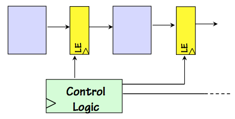 SGT System
The widely-used Synchronous Globally Timed engineering discipline depends upon a common
clock signal to synchronize the timing of signal transitions throughout the system; it
allows use of the single-clock synchronous timing scheme described in
Section 8.3.3.
Variants may partition the system into several clocking domains, each having its
own shared clock signal.
Individual components may have control signals, whose changes are synchronized
with the common clock.
A simple example is the
Load Enable input that dictates whether a register
loads new contents at the next clock edge.
The
globally-timed aspect of this approach reflects a centralized source
of these control signals, typically a FSM.
Synchronous Locally-timed Systems
11.8.3. Synchronous Locally-timed Systems
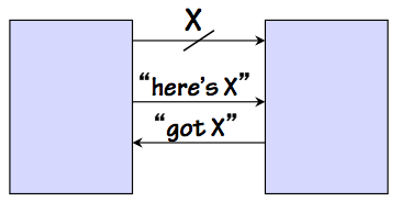
 Example SLT Protocol
Synchronous Locally-timed (or
self-timed) systems retain the shared clock,
and remain consistent with the single-clock discipline.
However, locally-timed systems involve a component-level signaling discipline by
which each component is told when to start an operation and reports when it has
finished, as shown to the left.
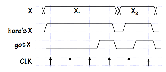 SLT Signal Timing
In this illustration, communication of data $X$ between two interconnected modules
is controlled by two signal lines: a "here's X" signal asserted by the source of
the $X$ data to indicate the cycle on which it becomes valid, and a "got X" response
from the recipient of $X$ to indicate that it has been safely loaded and no longer
must be asserted by the source.
A negative transition on "here's X" constitutes an acknowledgement that the
"got X" has been noted, and the $X$ value is no longer asserted.
In this example protocol, "got X" is asserted for a single cycle and
automatically returns to zero in the following cycle.
Because this is a synchronous protocol, each of these control signals must obey
setup and hold time constraints with respect to the common clock.
Locally-timed systems generally involve additional logic that combines
component timing signals to stimulate appropriate system-level timing.
A glimpse of such logic appears in
Section 11.8.4.1.
The elegant idea that underlies locally-timed systems is that the
time taken for each operation is determined by the component that performs
that operation, rather than by some externally specified plan.
Each component will begin a new operation when modules supplying input
data signal that the required inputs are ready, and will signal modules
depending on its output when the computation has completed.
Potential advantages of locally-timed system architectures include
- The timing of an operation, along with the implementation details
of that operation, are enclosed in a single component.
That component can be viewed externally as a "black box": knowledge
of its internal details and timing are unnecessary for its effective use
as a component. Thus, locally-timed component provides a more effective
abstraction than one whose timing details must be part of its specification.
- Upgrading a component of a locally-timed system with an improved,
faster version may improve the system performance with no additional
changes.
The new module will signal readiness of its output sooner, adjusting
the timing of subsequent operations automatically.
- A locally-timed component can exploit a more sophisticated timing
model than a conventional alternative.
The model may be data dependent: for example, a self-timed multiplier
might complete quickly when one of its operands is zero, allowing
system timing to exploit this shortcut without any external provision
in the system design.
For these and related reasons, self-timed protocols (both synchronous
and asynchronous) have enjoyed a cult following among the engineering
community, and are often utilized in situations where their abstraction
and adaptivity advantages are critical.
However, they come at some engineering cost: typically they replace timing
decisions that are made during the system design with logic that makes
these decisions dynamically during system operation, complicating
component design and imposing certain hardware and performance costs.
Asynchronous Locally-timed Systems
11.8.4. Asynchronous Locally-timed Systems
 Example ALT Protocol
Asynchronous locally-timed systems share the "have/got" control signals used
to handshake sequences of data along a data path, but abandon dependence on the
clock:
the detailed timing of the transfer is dictated by the timing of the control
signal edges themselves.
Typically the "have/got" signals follow a protocol similar to that described
for the synchronous locally-timed systems, where each of the control signals
makes both a positive and a negative transition for every data transfer in a
sequence.
This convention requires
two transitions on each control signal line
per transfer, imposing an engineering challenge since control signals change
at twice the frequency of the data values.
An elegant alternative is to use a
single transition signalling
protocol: the flow of data $X$ is controlled by a
"have X"/"got X" control signal pair where
any transition on
either control line -- positive or negative -- signals the corresponding
"have X" or "got X" event.
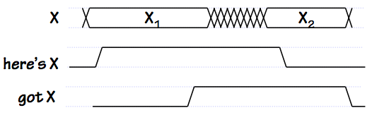 Single-transition Signalling
This scheme halves the frequency of control signal changes with respect to
the SLT protocol shown above: note, in the timing diagram to the right, a
single transition on each control signal for each new value of $X$ passed.
Locally-timed Example
11.8.4.1. Locally-timed Example
 Self-timed Example
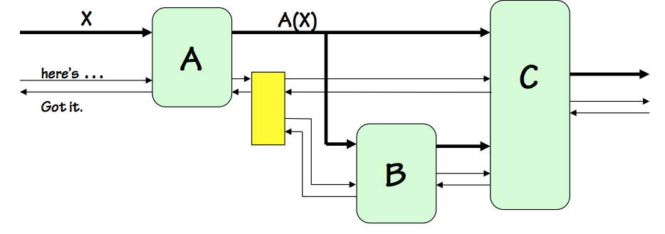
As a brief glimpse of the organization of a locally-timed system, consider
the Asynchronous Locally-Timed system shown to the right.
We assume an asynchronous (clockless) signaling scheme using
"have" and "got" signals that make two transitions to handshake each
data transfer, as described in
Section 11.8.3.
The system itself behaves as a locally-timed component following the same handshake protocol;
its input $X$ has "here's X" and
"got X" control lines to control the flow of data in, and its single output is
likewise associated with control signals in either direction to handshake data
to its destination.
Within the system itself, every data path has a pair of associated control signals
allowing the data source to signal readiness of the data, the destination to
signal readiness to accept the data, and so on.
Since the system components are locally-timed and follow the same protocol,
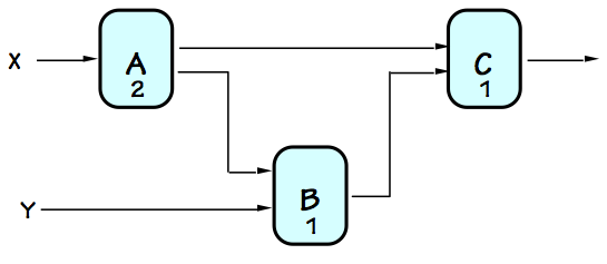
each internal data path is associated with a pair of "here's" and "got"
control signals between the source and destination of the data.
A complication arises from the output of the $A$ componenent, which is
routed to two destinations, $B$ and $C$.
The pair of control signals associated with $A$'s output must be routed
to control signal terminals of both the $B$ and $C$ modules, each a destination
whose timing must be coordinated with $A$'s output timing.
We show in the diagram a yellow box, representing a library
fan-out circuit module
associated with our timing discipline for routing a locally-timed data
path to multiple destinations.
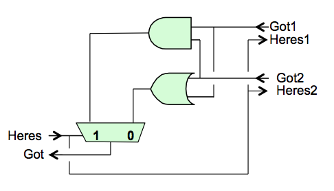 Fan-out Module
Plausible circuitry for this module is shown to the right.
The "have" signal for the source, asserted after the data output from $A$
has been made valid, can simply be routed to the destinations $B$ and $C$,
announcing that their respective input data are valid.
However, we require that $A$ maintain valid output data until
both
of these destinations have signaled that they no longer need it: a logical
AND of the acknowledgements by $B$ and $C$ that they have received the data.
The protocol requires the "got" signals to persist until the "here's" signal
is dropped, assuring that both input "got" signals will be present simultaneously
to generate the "got" output of the fan-out module.
Since the negative transition of the "got" signals indicated readiness for
new data, we need to combine the "got" signals from $B$ and $C$ in such a way
that $A$ sees a positive transition at the later of the two positive transitions,
and a negative transition at the later of the negative transitions on the
"got" signals from $B$ and $C$ as shown in the timing diagram to the left.
A computation of $C(A(X), B(A(X)))$ by our example locally-timed system would typically
proceed as follows:
- Initially the system is quiescent, and signals its readiness
to accept a new input by a logical 0 on the "got X" control signal
from $A$ to the component supplying $X$ data.
- When new $X$ data becomes available,
its source (connected to the $X$ data and control lines) drives valid input
data on the $X$ lines, and signals its readiness to $A$ via the "have X"
control signal.
- The $A$ component recognises that it has valid data, and begins
the computation of $A(X)$.
- At some point after seeing the "here's X" signal, $A$ will no longer
require valid input data and signal that via the "got X" line back to
its source.
This may happen early or late in the computation of $A(X)$, depending
on the design of the $A$ module (which may, for example, load the $X$
value into an internal register to allow a faster "got X" response).
- After the source of the $X$ data sees the "got X" signal, it will
return "here's X" to 0 and stop driving the $X$ data lines.
- Once the $A$ component has completed its computation, it drives
the $A(X)$ result on its output and signals its validity to the
$B$ and $C$ modules via the corresponding "here's" control signal.
- Seeing the signal that its $A(X)$ input data is valid, the
$B$ module begins its computation.
Once again, $B$ may respond with a "got A(X)" signal at any point
during its operation.
- When $B$ has computed $B(A(X))$, it drives its output line and
signals readiness to the $C$ module.
- The $C$ module begins its computation after it has been signaled
that its inputs from both $A$ and $B$ are ready.
Again, it may respond with the appropriate "got" control signals
at any point during its operation.
- When both $B$ and $C$ signal they no longer need their $A(X)$ input,
the fan-out logic signals "got A(X)" to $A$, which restores the "has A(X)"
signal to 0 and stops driving the $A(X)$ data lines.
- On completion of $C$'s computation, it drives its output data lines
and signals "here's C(A(X),B(A(X)))" to external components taking
this value as input.
Note that the order of these events is not necessarily fixed; modules
can vary the timing of their "got" control signals to input sources
as noted above.
This flexibility allows, for example, individual components to be
internally pipelined, so that a new $C(A(X),B(A(X)))$ computation
might be started in $A$ while the previous computation is still being
finished by the $B$ and $C$ components.
Chapter Summary
11.9. Chapter Summary
This chapter introduces two related but separate measures of the
performance of a system:
Latency, the end-to-end time
taken for each individual operation, and
Throughput,
the rate at which operations are performed.
These metrics can be used to characterize potential usefulness
of a wide range of systems, including combinational and sequential
digital information processing circuitry.
Latency and throughput of
parameterized
families of circuits, such as $N$-bit
adders, may be characterized in asymptotic terms as parameters
grow large using the $O(...)$ and $\theta(...)$ notations.
The latency of an $M$-word by $N$-bit ripple-carry adder, for example,
grows as $\theta(N+M)$.
Pipelining is introduced as a way of improving system throughput
at some cost in latency. A $k$-pipeline is a circuit having:
- $k$ distinct pipeline stages, separated by
registers on outputs of each stage;
- $k$ registers on every input-output path;
- potential to begin a new operation on each clock
cycle, producing corresponding outputs $k$ cycles later;
- Latency of $k \cdot t_{CLK}$ and throughput of $1 / t_{CLK}$,
where $t_{CLK}$ is the clock period.
Combinational circuits may be viewed as $0$-pipelines, a degenerate
case whose latency is $t_{PD}$ and whose throughput is $1 / t_{PD}$.