CMOS
6. CMOS
Having explored the powerful
combinational device abstraction
as a model for our logical building blocks, we turn to the search for
a practical technology for production of realistic implementations that
closely match our model. Our technology wish list includes:
- High gain and nonlinearity, as discussed in
Section 5.6, to maximize noise immunity.
- Low power consumption. Some power will be used as changing signal levels
cause current to flow in out out of parasitic capacitances, but an ideal
technology will consume no power when signals are static.
- High speed. Of course, we'd like our devices to maximize performance
(implying that $t_{pd}$ propagation delays be minimized and physical sizes
be small.
- Low cost.
During the few decades that electronic digital systems have exploded on
the engineering scene, a number of nonlinear device technologies have
been used -- ranging from electromagnetic relays to vacuum tubes and
diodes. The advent of semiconductor electronics and the miniaturization
push of integrated circuits, technology breakthroughs roughly contemporaneous
with the digital revolution, opened the way to incorporation of billions
of active devices (transistors) on the surface of a small silicon chip.
A remarkable succession of engineering improvements have allowed the
number of transistors on a chip to double roughly every two years for
the last 5 decades, a phenomenon popularly referred to as
Moore's Law
after its
observation
in 1965 by Intel founder Gordon Moore.
One technology,
CMOS (for
Complementary Metal-Oxide
Semiconductor), has emerged as the logic technology of choice,
getting high marks in each dimension of our wish list. We, like most
of industry, will focus on CMOS as our choice for implementing logic
devices.
MOSFETs
6.1. MOSFETs
The nonlinear circuit element in CMOS is the
MOSFET
or
Metal Oxide Semiconductor Field Effect Transistor,
whose physical structure is sketched below.
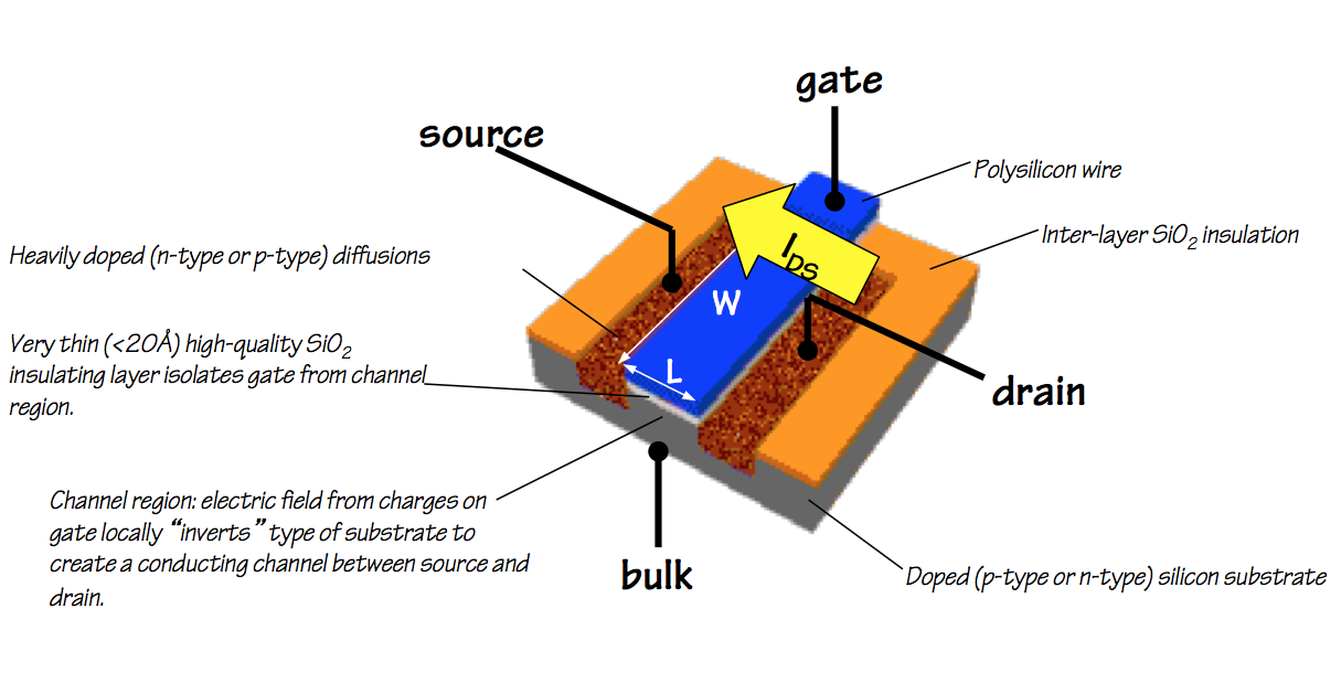 MOSFET physical layout
MOSFETs are used in CMOS logic as voltage-controlled switches:
current may or may not flow between two MOSFET terminals called
the
source and the
drain depending on the voltage
on a third terminal, the
gate, which separates them.
An important feature of MOSFETs is that no steady-state current flows between
the gate terminal and the source and drain: the gate behaves as if
it is coupled to the other terminals through a capacitor. Current flows
into and out of the gate terminal only when the gate voltage changes,
and then only until the charge on the gate reaches an equilibrium
that matches the voltage drop. This allows MOSFETs to draw no gate
current while quiescent (i.e., when logic values are constant);
if we design our CMOS circuits so that source
and drain currents of quiescent circuits are zero as well, we can
achieve the goal of zero quiescent power dissipation. We will adopt
shortly a cookbook formula that offers this major power advantage.
NFETs and PFETs
6.1.1. NFETs and PFETs
A key to CMOS circuit design is manufacturing technology that
allows fabrication of two different types of MOSFET on a single
silicon surface. The two flavors of transistor are the
N-channel and
P-channel FET, which perform
complementary functions in CMOS devices (hence the
C
in
CMOS).
Each FET is a four-terminal device; however our stylized use of
NFETs and PFETs involves connecting the $B$ (Bulk) terminal to
ground or $V_{DD}$ respecively, and using them as three-terminal
circuit components.
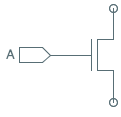
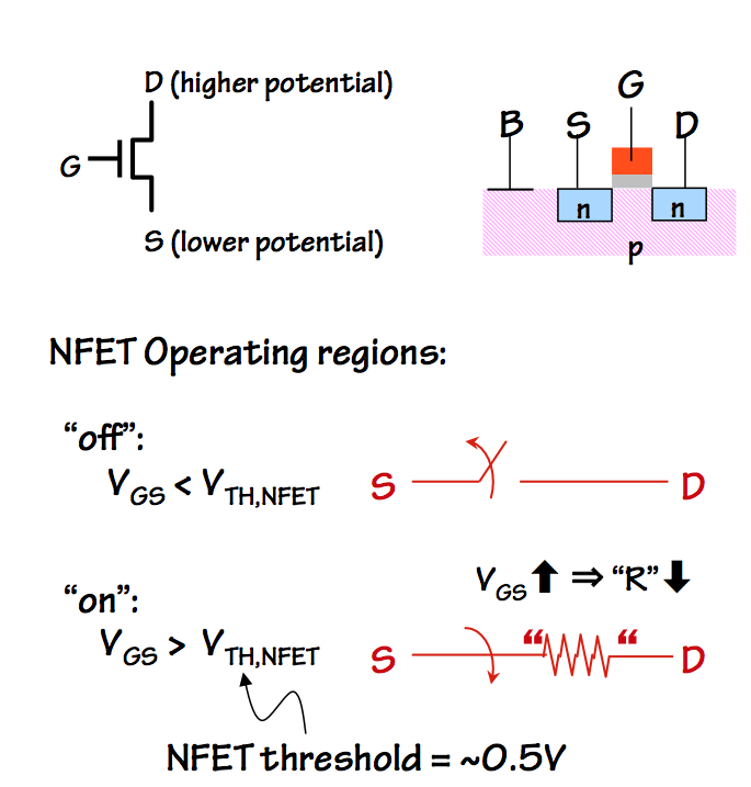 NFET switching behavior
The figure to the right shows the circuit symbol for an NFET, along
with a sketch of its physical layout and circuit models for its behavior
as a voltage-controled switch. The transistor is fabricated by embedding
n-type (doped) source and drain terminals in a p-type substrate, which
is connected to ground via the $B$ (Bulk) terminal.
The gate electrode controls the flow of current
between source and drain: if the voltage $V_{GS}$ between the gate and
the source is less than a threshold $V_{TH,NFET}$, no current flows
between source and drain: the transistor behaves like an open switch.
If $V_{GS}$ is above the $V_{TH,NFET}$ threshold, current flows from
drain to source, impeded by a small "on" resistance. A typical switching
threshold voltage is about a half volt. If we connect the source of an
NFET to ground, it provides an effective means of selectively grounding
the node connected to its drain by changing its gate voltage.
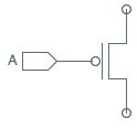
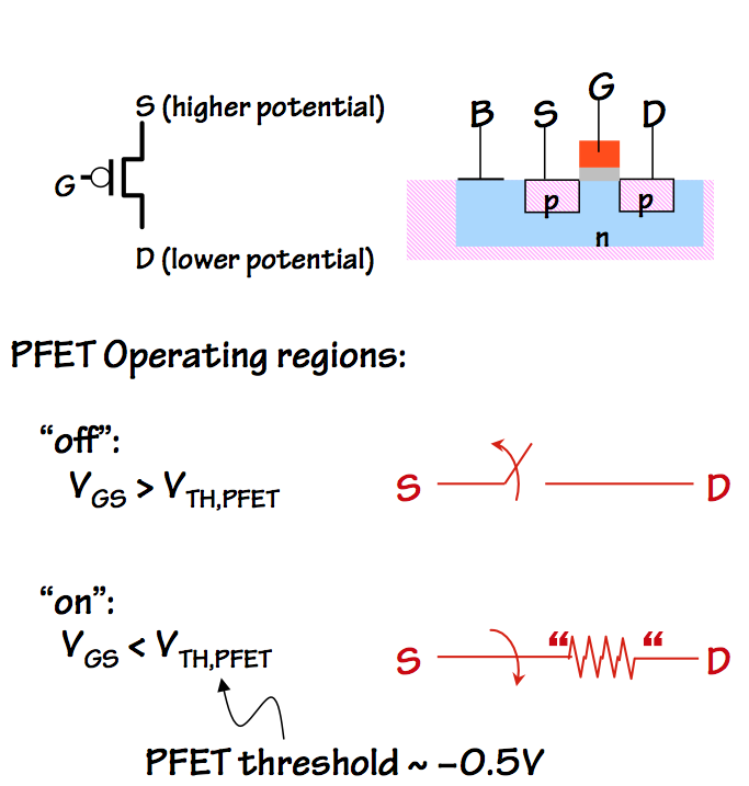 PFET switching behavior
The complementary PFET is made by embedding a well of n-type silicon
in the p-type substrate, and connecting the n-type well to the power
supply voltage $V_{DD}$ via terminal $B$ in the figure.
Within that well, the PFET transistor is
fabricated using opposite-polarity dopings from those of the NFET:
the source and drain are made of p-type silicon.
The circuit symbol for the PFET is similar to that of the NFET, with
the addition of an small circle at the gate terminal: these so-called
inversion bubbles are widely used in logic symbols to
indicate that the sense of a signal is opposite of what it would be
without the bubble. In the case of the PFET, it flags the fact that
the switch behavior is opposite of the NFET's: $V_{GS}$
above
a threshold value makes the PFET source/drain connection look like an
open switch, while $V_{GS}$ below the threshold connects source to
drain through a low "on" resistance. A PFET whose source is connected
to the power supply voltage $V_{DD}$ provides an effective way to selectively
connect its drain to $V_{DD}$.
Transistor Sizing
6.1.2. Transistor Sizing
Design parameters for each transistor include its physical
dimensions, which effect its current- and power-handling
capacity. It is common to parameterize FETs by the
width
and
length of the channel between the source and drain,
in scaled distance units:
length is the distance between source and drain, while width is
the width is the length of the channel/source and channel/drain
boundaries.
Of particular interest is the ratio between the
width and length of the channel, which determines
the "on" resistance and hence the current carrying capacity
of the source-drain connection when the transistor is "on".
In general, the drain-source current $I_{DS}$ is proportional
to the $Width/Length$ ratio.
While we will largely ignore transistor sizing issues in our
subsequent circuits, this parameter can play an important role
in the optimization of performance and energy consumption of
a digital circuit. A device whose output drives a long wire
or heavy capacitive load, for example, may benefit from tuning
of transistor sizes to provide higher-current output.
Pullup and Pulldown Circuits
6.2. Pullup and Pulldown Circuits
Each of the NFET and PFET devices behaves as a voltage-controlled switch,
enabling or disabling a connection between its source and drain terminals
depending on whether its gate voltage is above or below a fixed threshold.
Our intention is to select logic mapping parameters as described in
Section 5.4.1 that place the FET switching thresholds reliably
in the forbidden zone, so that valid logic levels applied to gate terminals
of NFETs and PFETs will open or close their source/drain connections.
By using logic levels to open and close networks of switches, we can
selectively drive
output terminals of logic devices to
ground ($0$ volts) or $V_{DD}$ (power supply voltage), which represent
maximally valid 0s and 1s respectively.
 Pullup/Pulldown circuits
In general, each logical output of a device will selectively connect to ground
through a
pulldown circuit and will selectively connect to $V_{DD}$
through a
pullup circuit, where the pulldown and pullup circuits
contain FETs whose gates are connected to logical inputs. Given our goals
of (a) driving each output to a valid logic level for each input combination
and (b) zero quiescent current flow, it is important that exactly one
of the pullup/pulldown circuits present a closed circuit for any input
combination. If neither circuit conducts, the output voltage will "float"
at some unspecified value, likely invalid; if both conduct, a low-resistance
path between $V_{DD}$ and ground will dissipate excessive power and likely
do permanent damage to the circuit.
NFETs are well suited for use in pulldown circuits since they
can connect the output terminal to ground potential via a small "on" resistance
but without a threshold voltage drop between the output voltage and ground;
for similar reasons, PFETs are a nearly ideal choice for use in pullup circuits.
Consequently CMOS combinational logic devices (commonly called "gates", not
to be confused with the gate terminal of a MOSFET) use only PFETs in pullup
circuits and NFETs in pulldowns. The main cleverness required in the design
of a CMOS gate is to come up with pullup and pulldown circuits that are properly
complementary -- that is, to design the circuits so that for every combination
of logical inputs, either the pullup or the pulldown is active but not both.
 CMOS
CMOS
Inverter
Recalling that an NFET is active (conducts) when its gate voltage is high
(a logic 1) and PFET is active when its gate voltage is low (a logical zero),
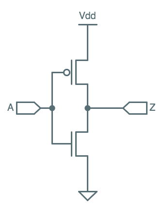
we can construct the simplest "interesting" CMOS gate: an inverter.
The inverter uses
a single PFET pullup and a single NFET pulldown as shown to the left.
Its logical input is connected to the gate terminals of both the PFET pullup
and the NFET pulldown, turning on the pulldown path when its value is 1 and
turning on the pullup path when its value is 0, causing the output voltage
to represent the opposite logic level from its input. We arrange that
$V_{il}$ is well below the switching threshold of both transistors, so that
a valid 0 input causes the pullup to conduct and the pulldown to present
an open circuit; similarly, ensuring $V_{ih}$ is well above the thresholds
assures the output terminal to be connected to ground and not $V_{DD}$ on
a valid 1 input.
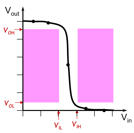 CMOS Inverter VTC
If we plot the voltage transfer curve of the CMOS inverter, we get something
like that shown to the right: the high gain near the switching thresholds
of the transistors is confined to the forbidden zone of our logic mapping,
neatly avoiding the shaded regions corresponding to invalid outputs caused
by valid inputs.
The pullup/pulldown architecture of CMOS gates assures that $V_{OH}$ and
$V_{OL}$ can be close to $V_{DD}$ and 0, respectively, while $V_{IL}$ and
$V_{IH}$ need only bracket the nearly vertical steps at the transistor
switching thresholds. This combination leads to good noise margins.
Recall that the voltage transfer curve represents an
equilibrium
output voltage for each input voltage.
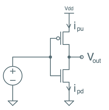 VTC Test Setup
It can be made using a test setup
similar to that shown on the left, where successive input voltages are
applied to our inverter input, and enough time is allowed to elapse to
let $V_{out}$ stabilize. Even with nothing connected to the output
terminal, this may take some time due to parasitic capacitances, resistances,
and inductances. At equilibrium, $V_{out}$ will be constant and $i_{pu} = i_{pd}$:
there will be no output current, so any current flowing through the pullup
must continue through the pulldown. Once this equilibrium is reached, $V_{out}$
is recorded on our voltage transfer curve and we move on to the next
input voltage.
Series and Parallel Connections
6.2.1. Series and Parallel Connections
Pullup and pulldown circuits for logic functions of multiple inputs
involves configuring series and parallel connections of PFETs (in
pullups) or NFETs (in pulldowns), again with each gate terminal
connected to one logical input.
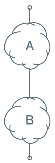
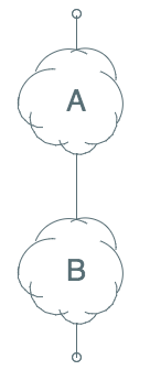
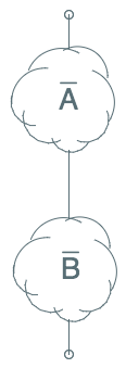
A quick review of parallel and series connection of "switching" circuits:
|
|
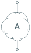
Assume that the notation shown to the left
represents a circuit that conducts when some circumstance we call $A$ is true,
and otherwise presents an open circuit between its two terminals.
|
|
|
Then the series circuit shown to the left
conducts only when both $A$ and $B$ are true: if either $A$ or $B$ is
false, the corresponding circuit will open and no current will flow. This
allows us to effect a logical AND between the conditions $A$ and $B$.
|
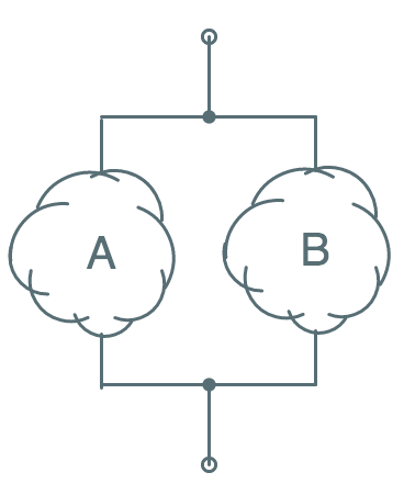
|
|
Similarly the parallel circuit
shown to the left
represents a circuit that conducts when either $A$ or $B$, or both $A$ and $B$,
are true. This effects a logical OR between the conditions $A$ and $B$.
|
Using series and parallel combinations of circuits containing NFETs and PFETs,
we can build pullup and pulldown circuits that are active -- pull an output
to ground or $V_{DD}$ -- based on ANDs and ORs of logic values carried on
input wires.
Complementary circuits
6.2.2. Complementary circuits
The remaining ingredient to our CMOS formula is the requirement that
we connect each output to
complementary pullups and pulldowns --
that is, that the pullup on an output is active on exactly the
combination of input values for which the pulldown on that output
is
not active.
| Circuit | Complement | Description |
|
|
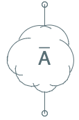
Notation:
The bar over the condition A indicates a circuit that is active
when $A$ is not true; thus the two circuits to
the left are complementary.
|
|
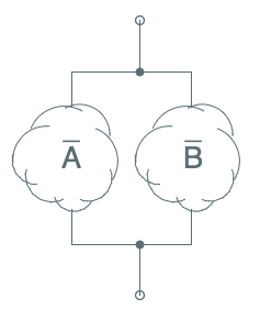
|
Given a series connection of circuits active on $A$ and $B$, we can construct its
complement by the parallel connection of complementary circuits $\bar A$ and $\bar B$.
|
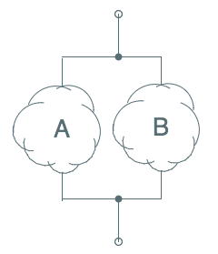
|
|
Given a parallel connection of circuits active on $A$ and $B$, we can construct its
complement by the series connection of complementary circuits $\bar A$ and $\bar B$.
|
|
|
Finally, we observe that an NFET connected to an input $A$ is the complement of a
PFET connected to the same input: the NFET presents a closed circuit when $A$ is
a logical 1, while the PFET closes when $A=0$ as we observed in the CMOS inverter.
|
The astute reader will notice that the above observations gives us a powerful
toolkit for building complementary pullup and pulldown circuits based on combinations
of input values. The NFET/PFET rule allows us to build pullups/pulldowns for
single variables, as we did in the inverter; the series/parallel constructions
allow us to combine pullups or pulldowns for several variables, say $A$ and $B$,
to make pullups or pulldowns for logical combinations such as the AND or OR of
$A$ and $B$.
Because of the electrical characteristics of PFETs and NFETs, CMOS gates
use only PFETs in pullup circuits and NFETs in pulldown circuits. Thus
each output of a CMOS gate is connected to a pullup circuit containing
series/parallel connected PFETs, as well as a complementary pulldown
circuit containing parallel/series connected NFETs.
It is worth observing that
- For every PFET-based pullup circuit, there is a complementary
NFET-based pulldown circuit and vice versa.
- Given a pullup or pulldown circuit, one can mechanically
construct the complementary pulldown/pullup circuit by systematically
replacing series with parallel connections, parallel with series
connections, PFETs with NFETs, and NFETs with PFETs.
The resulting ciruits are duals of one another,
and are active under complementary input combinations.
- Our restrictions to PFETs in pullups and NFETs in pulldowns
makes single CMOS gates naturally inverting: a logical 1
on an input can only turn on an NFET and turn off
a PFET. This limits the set of functions we can implement as
single CMOS gates: certain functions require multiple CMOS gates
in their implementation.
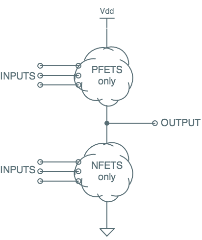
The CMOS Gate Recipe
6.3. The CMOS Gate Recipe
We use the term
CMOS gate to refer to a single-output combinational device
implemented as shown to the right. The output node is connected to $V_{DD}$
via a pullup consisting of zero or more PFETs, and is connected to ground via
a pulldown consisting of zero or more NFETs. The device has zero or more
logical inputs, and the gate terminal of each PFET or NFET is connected to
one such input.
In the typical CMOS gate,
- The pullup and pulldown circuits are duals of each other,
in the sense described in Section 6.2.2.
- Each input connects to one or more PFETs in the pullup, and
to an equal number of NFETs in the dual pulldown circuit.
An exception is the degenerate case of a CMOS gate whose
output is independent of one or more inputs; in this case, the
ignored inputs are not connected to anything.
- For the above reasons, a single CMOS gate typically comprises
an even number of transistors, with equal numbers of NFETs and
PFETs.
Our specification of "zero or more" transistors in the pullup/pulldown
circuits allows us to include the degenerate extremes as CMOS gates:
devices which ignore
all their inputs and produce a constant
0 or 1 as output by connecting the output node to $V_{DD}$ or ground.
In general, we can approach the design of a CMOS gate for some simple
function F by either
- Designing a pulldown circuit that is active for those input
combinations for which $F=0$, or
- Designing a pullup circuit that is active for those input
combinations for which $F=1$
and then systematically deriving the complementary pullup/pulldown
circuit by taking the dual of the circuit we've designed. Finally,
we combine them to make the CMOS gate per the above diagram.
Common 2-input gates
6.3.1. Common 2-input gates
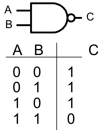 NAND gate
A simple application of the above recipe can be used to implement
the popular 2-input
NAND gate, whose circuit symbol and
truth table are shown to the right. The name
NAND derives
from "Not AND", reflecting the fact that the gate's output is the
inverse of the logical
AND of its two inputs. The circuit
symbol, similarly, consists of a shape conventionally used to depict an
AND
operation -- having a straight input side and a curved output side --
with a small circle (or
bubble) at its output which
conventionally denotes inversion.
From the NAND truth table, we observe that the gate output should
be zero if and only if both input values are 1, dictating a pulldown
that is active (conducting) when the A and B inputs both carry a high
voltage.
 CMOS NAND gate
The pulldown is handily constructed from a series-connected pair of NFETs between
the output node and ground, as shown in the diagram to the left.
The complementary pullup circuit is the dual of the pulldown, consisting
of parallel-connected PFETs between the output C and the supply voltage $V_{DD}$,
again as shown in the diagram. The gate element of each FET in the pullup
and pulldown circuits is connected to one of the logical inputs ($A$ or $B$)
to our CMOS gate, causing logical input combinations to open and close the
FET switches effecting an appropriate connection of the output $C$ to $V_{DD}$
or ground according to the values in the truth table.
 NOR gate
Alternatively, the use of parallel-connected NFETs in the pulldown and series-connected PFETs in the pullup
yields a CMOS implementation of the
NOR gate whose circuit symobl and truth table are shown to the right.
 CMOS NOR gate
Again, the symbol is a composite of the standard symbol for a logical
OR with
an inversion bubble on its output, indicating a "Not OR" or
NOR operation.
The corresponding CMOS implementation is shown to the left.
The CMOS implementation of a 2-input NAND gate can be easily extended
to NAND of 3-, 4- or more inputs by simply extending the series pulldown
chain and parallel pullup with additional FETs whose gate elements
connect to the additional logical inputs.
Similarly, the 2-input NOR gate can be extended to 3 or more input NOR
operations by adding an NFET/PFET pair for each additional logical input.
Electrical considerations
(such as delays due to parasitics) usually limit the number of inputs of single
CMOS gates (the so-called
fan-in) to a something like 4 or 5;
beyond this size, a circuit consisting of several CMOS gates is likely
to offer better cost/performance characteristics.
Properties of CMOS gates
6.4. Properties of CMOS gates
The CMOS gate recipe of an output node connected complementary PFET-based pullup
and NFET-based pulldown circuits offers a nearly ideal realization of
the
combinational device abstraction, since
- For each input combination, it will drive its output to an
equilibrium voltage of 0 (ground) or $V_{DD}$, generating ideal
representations of logical $0$ or $1$.
- At equilibruim, the FETs used in the pullup/pulldown circuits
draw zero gate current. This implies that CMOS gates draw zero
input current once parasitic capacitances have been charged to
equilibrium, hence CMOS circuits have zero static power dissipation.
In the following sections, we will explore additional consequences of
the CMOS gate design regimen.
CMOS gates are inverting
6.4.1. CMOS gates are inverting
It may seem peculiar that the example CMOS gates chosen for
Section 6.3.1 include
NAND and
NOR
but not the conceptually simpler logical operations
AND and
OR. In fact, this choice reflects a fundamental constraint
of CMOS: only certain logical functions --
inverting functions --
can be implemented as a single CMOS gate. Other functions may be implemented
using CMOS, but they require interconnections of multiple CMOS gates.
To understand this restriction, consider the effect of an input to
a CMOS gate on the voltage on its output node. A logical $0$ -- a
ground potential -- can only affect the output by turning
off
NFETs in the pulldown and turning
on PFETs in the pullup,
forcing the output to a logical $1$. Conversely, an input $1$
can only effect the output voltage by driving it to a logical $0$.
This constraint is consistent, for example, with a k-input
NOR
operation, where a $1$ on any input forces the output to become $0$;
however, it cannot represent a logical $OR$, where a $1$ on any input
must force the output to become a $1$. Thus we can implement k-input
NOR as a single CMOS gate, but to implement k-input
OR
we use a k-input
NOR followed by an inverter.
We can determine whether a particular function F can be implemented as
a single CMOS gate by examining pairs of rows of its truth table that
differ in only one input value. Changing an input from $0$
to $1$ can only effect a $1$-to-$0$ change on the output of a CMOS gate,
or may leave the output unchanged; it cannot cause a $0$-to-$1$ output
change. Nor can a $1$-to-$0$ input change cause a $1$-to-$0$ output
change.
Thus the observation that $F(0,1,1)=1$ but $F(0,0,1)=0$ causes us to
conclude that the function $F$ cannot be implmented as a single CMOS
gate.
To generalize slightly, suppose that we
know that some
3-input function $F$ is implemented as a single CMOS gate, and that
$F(0,1,1)=1$. Since changing either of the input $1$s to $0$ can
only force the output to become $1$, that implies $F(0,x,y)=1$
for
every choice of $x$ and $y$, an observation that we
might denote as $F(0,*,*)=1$ using $*$ to denote an unspecified
"
don't care" value. Similarly, knowing that $F(1,0,1)=0$
implies that $F(1,*,1)=0$ since changing the second argument from $0$
to $1$ can only force the already-$0$ output to $0$.
Knowing that the output of a CMOS gate is $0$ for some particular
set of input values assures us that the $1$s among its inputs are
turning on a set of NFETs in its pulldown that connects its output
node to ground: its output will be zero so long as these input $1$s
persist, independently of the values on the other inputs. Similarly,
knowing that a CMOS gate output is $1$ for some input combination
assures us that the $0$s among the inputs enable a pullup path
between the output and $V_{DD}$, independently of the other inputs.
Taking these observations to the extreme, a CMOS gate whose output
is $1$ when all inputs are $1$ can only be the degenerate gate whose
output is always $1$ independently of its inputs, and similarly for
the gate whose output is $0$ given only $0$ input values.
CMOS gates are lenient
6.4.2. CMOS gates are lenient
We can take the observations of the previous section one step further
to show that CMOS gates are
lenient combinational devices
as described in
Section 5.9.2.
Recall that lenience implies the additional guarantee of output validity
when a
subset of the inputs have been stable and valid for $t_{PD}$, so
long as that input subset is sufficient to determine the output value.
For example, if the truth table of a 3-input lenient gate $G$ specifies
that $G(0, 0, 1) = 1 = G(0, 1, 1)$, which we abbreviate as $G(0, *, 1) = 1$,
then $G$'s lenience assures that its output will be $1$ whenever its first
input has been $0$ and its third input has been $1$ for at least $t_{PD}$,
independently of the voltage (or validity) of its second input.
If $G$ is implemented as a single CMOS gate, this lenience property
follows automatically. In our example, the $G(0, *, 1) = 1$ property of
the truth table dictates a pullup with a path that connects the output
to $V_{DD}$ whenever the first input is $0$,
viz. a PFET gated
by the first input between the output node and $V_{DD}$. This connection
is independent of the second input as dictated by the truth table, and
is in fact independent of the third input since PFET paths can only be turned
on by $0$ inputs. Because of the complementary nature of the pulldown
circuitry, a $0$ value on $G$'s first input must turn
off an
NFET in every path between the output node and ground, disabling the
pulldown. Thus a $0$ on the first input electrically connects the output
node to $V_{DD}$ independently of the voltages on the other two inputs:
they may represent valid $0$, valid $1$, or be invalid (in the forbidden zone).
An analogous argument can be made for a CMOS gate $G$ whose value is $0$
(rather than $1$)
for some subset of input values, e.g. if $G(0, *, 1) = 0$. In this
case, $G$'s output must be connected to ground via
some NFET in the pulldown gated by the third input, and that connection
is assured by the $G(*, *, 1)$ input pattern independently of the
voltages on the first two inputs.
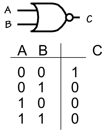
NOR gate
As a concrete example, consider the functional specification of
a 2-input NOR gate shown to the right.
 NOR glitch
Consider an experiment where we hold one input -- $A$ -- of the NOR
gate at a logical $1$, and make a transition on the other input from $1$
to $0$ as shown in the diagram to the left.
Consulting the NOR truth table, both the initial output of the gate
(prior to the input transition) and its final output should be $0$.
Assuming only that the gate
obeys the specifications as a combinational device,
the output $C$ is constrained to be $0$ until $t_{CD}$ following the input
transition, and again $t_{PD}$ after the transition; however, it is completely
unspecified between the ends of the $t_{CD}$ and $t_{PD}$ windows. During this
time it may exhibit a "glitch", even becoming a valid $1$ multiple times, before
settling to its final value of $0$.
This behavior is completely consistent with the combinational device
abstraction, and is usually unobjectionable in practice. But consider
repeating the above experiment using our CMOS implementation of NOR,
shown to the right.
The connection of the $A$ input to a constant $1$ has the effect of
turning off one of the series-connected PFETs in the pullup, isolating
the output from $V_{DD}$; it also turns on one of the parallel-connected
NFETs in the pulldown, assuring a connection between the output and ground.
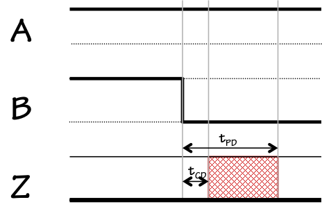 Lenient NOR timing
The $A=1$ constraint thus assures an output of $0$
independently of
the input $B$, which can be either logic value (or invalid) without compromising
the output so long as $A$ remains $1$. In addition to obeying the rules
for a combinational device, the CMOS implementation is lenient: its output
validity is assured by any subset of inputs sufficient to determine an output
value, and is uneffected by changes on other inputs.
Generalizing,
if we consider various paths through the pullup and pulldown
circuits of a CMOS gate we can systematically constuct rows
of a lenient truth table (containing
don't-care inputs, written as $*$).
Each path between the output and ground through the pulldown circuit
determines a set of inputs (those gating the NFETs along the path)
capable of forcing the output to $0$; similarly, each path through
the pullup circuit determines a set of inputs capable of forcing a $1$
output. Whenever the inputs along a pullup path are all $0$ the gate
output will be $1$, and whenever the inputs along a pulldown path are
all $1$ the gate will output a $0$. Each of the pullup paths corresponds
to a truth table line whose inputs are $0$s and $*$s and whose output is $1$;
each of the pulldown paths corresponds to a line with $1$ and $*$s as inputs
and a $0$ output. In general, the behaviour of every single CMOS gate
can be described by a set of such rules, and conforms to our definition
of a lenient combinational device.
It is important to note that, while every single CMOS gate is lenient,
combinational devices constructed as circuits whose components are
CMOS gates are not necessarily lenient.
This topic will be revisited in
Section 7.7.1.
CMOS gate timing
6.4.3. CMOS gate timing
As
combinational devices, the timing of a CMOS gate is
characterized by two parameters: its propagation delay $t_{PD}$,
an upper bound on the
time taken to produce valid outputs given valid inputs, and its
contamination delay $t_{CD}$, a lower bound on the time elapsed
between an input becoming invalid and the consequent output invalidity.
The physical basis for these delays is the time required to change
voltage on circuit nodes due to capacitance, including the unavoidable
parasitic capacitance discussed in
Section 4.3.1.
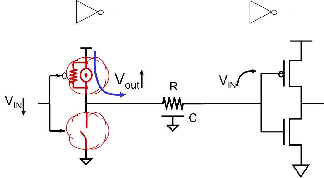
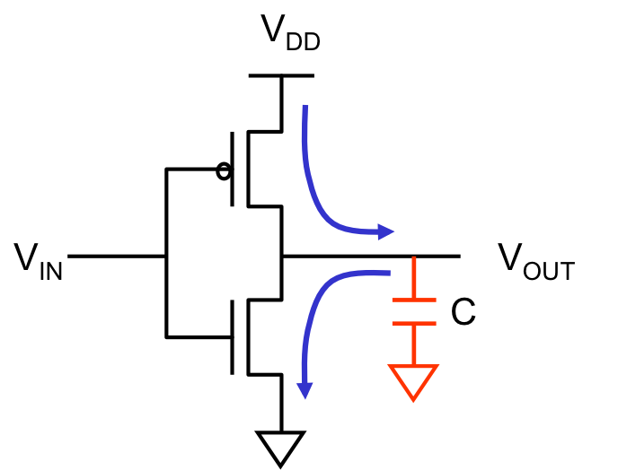
Consider a CMOS inverter whose output connects to another inverter,
as shown to the right. The output node is characterized by some
capacitive load, $C$, which includes both intrinsic capacitance of
connected inputs as well as parasitic capacitance of the wiring.
When the input $V_{IN}$ to the left inverter
makes a transition from $1$ to $0$, it enables current to flow through
the pullup to the output node and charge this capacitance, at a rate
proportional to the current flow through the enabled pullup.
This current is
limited by the non-zero
on resistance of the enabled PFET, as
well as parasitic resistance of the wiring itself.
The result is an exponential rise of the output voltage toward $V_{DD}$
whose time constant is the product of the capacitance $C$ and the resistance,
much like the example of
Section 4.3.1.
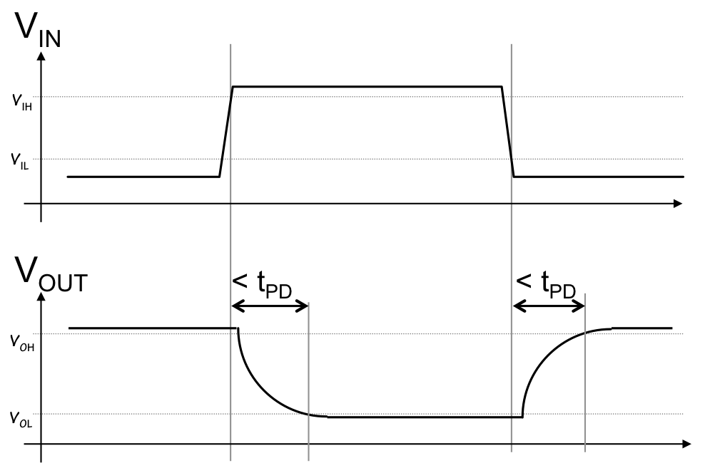
When a device output changes from a logical $0$ to a logical $1$, we will
observe an exponential rise or fall toward the target value; we often refer
to the time taken for this curve to go from a valid $0$ to a valid $1$ as
the
rise time of the signal, and to the timing of its opposite
transition as the
fall time. There will typically be a brief
delay prior to the rise or fall time corresponding to the propagation of
a changed input value through the affected pullup and pulldown transistors
as shown to the right.
Delay specifications
6.4.4. Delay specifications
The
combinational device abstraction of
Chapter 5,
based as it is on the idealized circuit theoretic model of components connected
by equipotential nodes, requires that we bundle the timing behavior discussed in the prior
section into the $t_{PD}$ and $t_{CD}$ timing specifications of devices driving
each digital output node.
The contamination delay $t_{CD}$ specifies a
lower bound on the time a
previously-valid output will remain valid after an input change; we choose this
parameter to conservatively reflect the minimum interval required for an input
change to propagate to affected transistors and begin their turnon/turnoff transition.
Often we specify contamination delay as zero, which is always a safe bound; in
certain critical situations, we choose a conservative non-zero value to guarantee
a small delay between input and output invalidity.
Since the propagation delay $t_{PD}$ specifies an upper bound on the time between an input stimulus
and a valid output level, it should be chosen to conservatively reflect the maximum
delay (including transistor switching times and output rise/fall times) we anticipate.
We might make this selection after testing many samples under a variety of output
loading and temperature circumstances, extrapolating our worst-case observations to
come up with a conservative $t_{PD}$ specification.
The $t_{PD}$/$t_{CD}$ timing model gives our digital abstraction simple and
powerful analysis tools, including the ability to define provably reliable
combinational circuits (the subject of
Section 5.3.2) as
well as sequential logic (
Chapter 8).
However, it squarely confronts the major dilemma previewed in
Section 4.5.2: the abstraction of
space from the
circuit-theoretic model of signal timing.
In practice, the timing of the output of a CMOS gate depends not only
on intrinsic properties of the gate itself, but also on the electrical
load placed on its output by connected devices and wiring. The delay
between an input change to an inverter and its consequent valid output
cannot realistically be bounded by an inverter-specific constant: it depends
on the length and routing of connected wires and other device inputs.
The fact that wire lengths and routing are determined late in the
implementation process distinguishes these factors as implementation
details rather than properties of a specified digital circuit, a fact
that simply violates the constraints of our digital circuit abstraction.
Fortunately, the properties of CMOS as an implementation technology
offer opportunities to reach a workable compromise between the simplicity
and power of our propagation-delay timing model and realistic physics
of digital systems. In particular, the fact that CMOS devices draw
no steady-state input current implies that the output of a CMOS gate
will eventually reach its valid output value; its simply not practical
to bound the time this will take without consideration of wiring
and loading details. Thus we can design circuits using "nominal"
values for $t_{PD}$ specifications -- chosen using light loading --
and design circuits that will operate properly but whose overall
timing specifications may turn out to be optimistic once wiring
is taken into account.
In
Section 8.3.3, we describe
an engineering discipline for designing systems with a single
timing parameter -- a
clock period -- that controls the
tradeoff between computational performance and the amount of time
allowed for signals on every circuit node to settle to their target
values. Systems we design using this discipline will be guaranteed
to work for
some (sufficiently slow) setting of this parameter,
as sketched in
Section 4.5.2.1.
We will revisit this issue in later chapters. For now, we will
assign nominal propagation delays to devices, and design and
analyze our circuits using the fictitious promise made on their
behalf by the combinational device abstraction.
Power Consumption
6.5. Power Consumption
An attractive feature of CMOS technology for digital systems is
the fact that, once it reaches a static equilibrium and all circuit
nodes have settled to valid logic levels, no current flows and
consequently no power is dissipated. This property implies that
the power consumption of a CMOS circuit is proportional to the rate
at which signals
change logic levels, hence -- ideally --
to the rate at which useful computation is performed.
The primary cause of current flow within a CMOS circuit is the
need to charge and discharge parasitic capacitances distributed
among the nodes of that circuit, and the primary mechanism for
energy consumption is the dissipation of energy (in the form of
heat) due to ohmic losses as these currents flow through the incidental
resistances in wires and transistors.
Consider, for example, the operation of the CMOS inverter shown to the right
as its input voltage switches from a valid $0$ to a valid $1$ and back again
to a valid $0$. The output node is inevitably coupled to ground (as well as
$V_{DD}$ and perhaps other signal wires) by some parasitic capacitance, shown
in the diagram as a lumped capacitor to ground.
If the initial $V_{IN}$ is zero (corresponding to a valid logical $0$),
the equilibrium $V_{OUT}$ is $V_{DD}$; at this static equilibrium, no
current flows, but the charged capacitor has a stored energy of $C\cdot V_{DD}^2/2$
joules, where $C$ is the total capacitance.
If $V_{IN}$ now makes a transition to $V_{DD}$ (a valid $1$), the pullup
PFET opens and the pulldown closes, providing a low-resistance path between
the output node and ground; the capacitance discharges through this path,
until it reaches its new equilibrium $V_{OUT}=0$. The capacitor now has
been discharged to zero volts: it has lost the $C\cdot V_{DD}^2/2$ joules of
energy it previously stored. This energy has in fact been converted to
heat by the flow of current through the resistance along its discharge
path.
A subsequent $1 \rightarrow 0$ transition on $V_{IN}$ will open the pulldown
and close the pullup, charging the output capacitance back to $V_{DD}$ and
dissipating another $C\cdot V_{DD}^2/2$ joules by ohmic losses from the necessary
current flow. The total energy dissipation from this $0 \rightarrow 1 \rightarrow 0$
cycle is $C \cdot V_{DD} ^2$ joules.
Similar energy losses occur at each node of a complex CMOS circuit, at rates
proportional to the frequency at which their logic values change.
If we consider a system comprising $N$ CMOS gates cycling at a frequency
of $f$ cycles/second, the resulting power consumption is on the order of
$f \cdot N \cdot C \cdot V_{DD} ^ 2$ watts.
As a representative example, a CMOS chip comprising $10^8$ gates driving
an average output capacitance of $10^{-15}$ farads using $V_{DD} = 1$ volt
and operating at a gigahertz ($10^9$) frequency would consume about
$10^8 \cdot 10^9 \cdot 10^{-15} \cdot 1^2 = 100$ watts of power, all
converted to heat that must be conducted away from the chip.
The constraint of power (and consequent cooling) costs has been a prime
motivator for technology improvements. Historic trends have driven
the number of gates/chip higher (due to Moore's law growth in transistors
per chip), and -- until recently -- operating frequencies have increased
with each generation of technology. These trends have been partially
offset by scaling of CMOS devices to smaller size, with proportionate
decreases in capacitance. Lowering operating voltage has been a
particular priority (due to the quadratic dependence of power on
voltage), but the current 1 volt range may be close to the lower limit
for reasons related to device physics.
Must computation consume power?
6.5.1. Must computation consume power?
The costs of energy consumption (and related cost of cooling) have
emerged as a primary constraint on the assimilation of digital technologies,
and are consequently an active area of research.
A landmark in the exploration of fundamental energy costs of computation
was the
1961 observation by Rolf Landauer
that the act of
destroying a single bit of information
requires at least
$k \cdot T \cdot ln 2$ joules of energy, where $k$ is the Boltzmann constant
($1.38 \cdot 10^{-23}$ J/K), $T$ is the absolute temperature in degrees Kelvin, and $ln 2$
is the natural logarithm of $2$.
The attachement of this lower limit to the
destruction of information
implies that the cost might be avoided by building systems that are
lossless
from an information standpoint: if information loss implies energy loss,
a key to energy-efficient computations is to make them preserve information.
Landauer and others proposed that low-energy computations be performed using only
information-preserving operations.
They observed that for common functions like NAND or the
exclusive-or (XOR) shown to the left -- comprising 2 bits of input
information but producing a single output bit -- information is necessarily lost:
the inputs cannot be reconstructed from the output values. Consequently on each
XOR operation some information is lost, with the consequent accrued energy cost as
dictated by the Landauer limit.
If however we restrict our basic logical operations to information-preserving functions
like the Feynman gate shown to the right, and carefully preserve all output information
(even that not required for our computation), we might avoid this energy penalty.
Note that the $Q$ output of the Feynman gate carries the same information as the
output of the XOR gate, but the additional $P$ output disambiguates the input
combination generating this output.
Landauer and his disciples observed that such lossless computation can be
made
reversible: since no information is lost in each step of the computation,
it may be run backward as well as forward.
Although construction of a completely reversible computer system presents some
interesting challenges (e.g. input/output operations), it is conceptually
feasible to perform arbitrarily complex computations reversibly. Imagine,
for example, an intricate and time-consuming analysis that produces a valuable
single-bit result. We start this computation on a reversible computer in some
pristine initial state, perhaps with a large memory containing only zeros.
As the computation progresses using reversible operations, extraneous outputs
are saved in the memory, which gradually fills with uninteresting data.
During this process, we may pump energy into the computer to effect its
state changes, but theoretically none of this energy is dissipated as heat.
When we have computed our answer, we write it out (irreversibly) at a tiny
energy cost. We then run our computation in reverse, using the stored
extraneous data to step backwards in our computation; in the process, we
get back any energy we spent during the forward computation. When the
backward phase is completed, the machine state has been returned to its
pristine initial state (ready for another computation), we have our
answer, and the only essential energy cost has been the tiny amount needed
to output the answer.
Such thought experiments in reversible computation seem (and are) somewhat
far-fetched, but provide important conceptual models for understanding
the relation between laws of physics and those of information. Reversible
computing plays an important role in contemporary research, for example
in the area of quantum computing.
Further Reading
6.6. Further Reading
-
Moore, G., "Cramming More Components onto Integrated Circuits",
Electronics, v 36 no 8, April 19, 1965.
1965 paper observing that the optimal transistor count for a chip
seemed to double ever two years, and predicting that growth rate
to continue for "at least 10 years". This conservative prediction
predates the popularity of CMOS (and many other subsequent technological
breakthroughs), and has come to be known as Moore's Law.
-
Landauer, Rolf, "Irreversibility and heat generation in the computing process",
IBM J. Research and Development, 1961.
1961 paper exploring the theoretical limit of energy consumption of computation.
Establishes a lower bound on the energy cost of erasing a bit of information,
and hence of irreversible computation.
Chapter Summary
6.7. Chapter Summary
The CMOS technology described in this chapter has become the tool of
choice for implementing large digital systems, and for a number of
good reasons:
- Effective manufacturing techniques allow economical manufacture
of reliable devices containing billions of logic elements;
- Quiescent CMOS circuits have virtually zero power dissipation;
- CMOS gates are naturally lenient combinational devices.
Key elements of the CMOS engineering discipline include:
- The use of complementary transistor types, NFETs and PFETs,
within each CMOS gate;
- Each CMOS output is a circuit node connected to an NFET-based
pulldown circuit as well as a PFET-based pullup
circuit, where for every combination of inputs either the pullup
connects the output to $V_{dd}$ or the pulldown connects the
output to ground;
- Each single CMOS gate is naturally inverting: positive input
transitions can cause only negative output transitions, and vice
versa. Hence certain
logic functions cannot be implemented as a single CMOS gate
and require multiple-gate implementations;
- High gain in the active region allows large noise margins,
hence good noise immunity.
- Transitions take time: pumping charge into or out of an
output node is work (in the physical sense) and cannot happen
instantaneously. This leads to finite rise and fall times,
which we accommodate in our $t_{pd}$ specifications.
Although single CMOS gates are naturally lenient, we observe
that acyclic circuits of CMOS gates are not necessarily lenient.
If lenience is required of a CMOS circuit, it can be assured
by an appropriate design discipline.