
The Digital Abstraction
5. The Digital Abstraction
Having explored ways to use a binary channel capable of transferring bits between a transmitter and receiver, we now turn to the problem faced by the channel itself: physical representation of individual ones and zeros in a form that allows them to be manipulated and communicated reliably. In dealing with this problem, we will confront the deceptively complex problem of representing discrete variables as continuously-variable physical quantities; moreover, we will establish one of the major abstractions of digital systems: the combinational device.Why digital?
5.1. Why digital?
In classical physics, measureable quantities that we might use to represent information -- position, voltage, frequency, force, and many others -- have values that vary continuously over some range of possibilities. The values of such variables are real numbers: even over a restricted range, e.g. the interval between 0 and 1, the number of possible values of a real variable is infinite, implying that such a variable might carry arbitrarily large amounts of information. This may appear as an advantage of continuous variables, but it comes at a serious cost: it obscures the actual information content of the variable. This limitation of the engineering discipline surrounding analog systems results in symptoms like the degraded video content of our video toolkit example of Section 4.4.Role of Specifications
5.1.1. Role of Specifications
Informally, engineering involves building things: assembling components to make a system that performs some useful function. We formalize this process via specifications, both for the system and its components. Specifications abstract the external function performed by a module, and isolate that function from the internal details of the module's implementation. Ideally, a module's specifications provide all of the information an engineer using that module as a component needs to know, without encumbering that user-level view with details relevent to the implementation of the module. Given well-designed specifications, the engineering of a system becomes the task of finding an arrangement of interconnected components that is guaranteed to meet the system specification, assuming that each of the component modules meets its module specification. Well-engineered systems are tantamount to a proof that the system "works", assuming that each of the modules work, where our standard of working is set by the specifications. While the proof is rarely formalized explicitly, it is implicit in the choices made by the system's designer. If we are to build systems of arbitrary complexity, it is important that specifications of each module characterize that module's behavior -- viz., the information flowing into and out of each module -- precisely rather than approximately. Specifications that can only be approximated in real-world implementations, such as those for our analog video toolkit, result in systems that obey their specifications only approximately; as these systems are combined to make yet bigger systems, the approximations continue to degrade. Such models can and are used for systems of limited complexity; but to remove this complexity limit, we need an abstraction whose specifications can be simply and precisely realized in practice.Representing discrete values: Part 1
5.2. Representing discrete values: Part 1
An enabling step toward the goal of simple, precisely realizable specifications is to adopt an abstract model based on discrete rather than continuous (real) variables. Although other possibilities exist, we choose the binary symbols $\{0, 1\}$ as the two distinct values that each variable may assume, so that each variable carries at most a single bit of information. The move from the unbounded information content of a continuous variable to the finite -- indeed tiny -- single bit of a binary variable represents a serious compromise in the capabilities of our model: it implies, for example, that each module's inputs and outputs each carry finite information. Paying that price, however, allows us to build devices whose specifications are obeyed precisely, and to combine the devices (and their specifications) to build systems of arbitrary complexity that obey their specifications precisely. Given that the real-world physical variables we must use to implement our devices use continuous variables, translating our discrete-value models to real-world implementations requires a scheme for representing discrete values as real quantities like voltage. We must somehow represent 0 and 1 as distinct quantities, with no intermediate alternatives. Moreover, we must assure that the representation of a 0 is never mistaken for a 1, and vice versa. In an electronic system whose wires carry voltages between 0 and 1, we might choose that voltage less than $0.5v$ represent 0 and those above $0.5$ represent 1; however, then voltages arbitrarily close to the $0.5v$ threshold could easily be misinterpreted.
Simple binary representation
Combinational Devices
5.3. Combinational Devices
Armed with a plausible approach to implementing the digital (discrete) $\{0, 1\}$ values of our model, we now introduce an abstraction for its major building block: A combinational device is a component that has- one or more digital inputs;
- one or more digital outputs;
- a functional specification that details the logic value of each output for each combination of input values;
- a timing specification consisting, at minimum, of a propagation delay: an upper bound $t_{pd}$ on the time required for the device to compute the specified output values from an arbitrary set of stable, valid inputs.
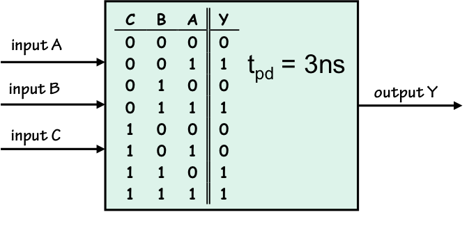
Combinational Device
The Static Discipline
5.3.1. The Static Discipline
The specifications of a combinational device represent a contract between that device and its system context:-
each output will be the valid logic value
dictated in its specifcation whenever its inputs have been valid for at least
the specified propagation delay.
Combinational Circuits
5.3.2. Combinational Circuits
A compelling property of the combinational device abstraction as a building block is the ability to build complex combinational devices by combining simpler ones. In particular, we can specify a new combinational device $S$ by a diagram of interconnected components such that- Each component is itself a combinational device;
- Each component input is connected to either
- an input to the system $S$;
- an output of another component; or
- a constant $0$ or $1$.
- Each output of the system $S$ is connected to either
- an input to the system $S$;
- an output of a component; or
- a constant $0$ or $1$.
- The circuit contains no directed cycles, i.e, there is no cyclic path within the diagram that goes from inputs to outputs through one or more components.
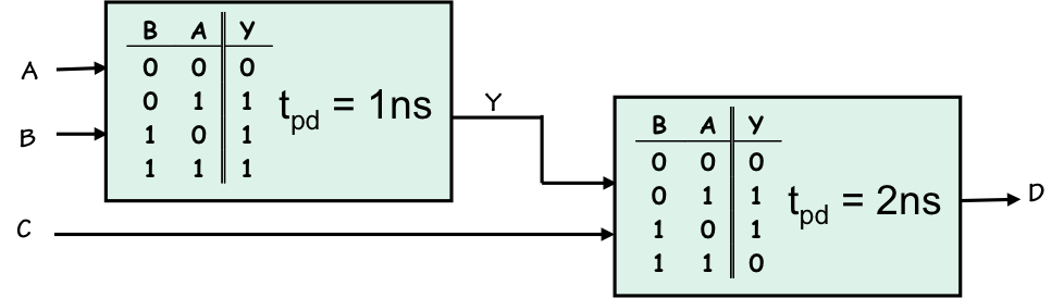
- Consider each path from an input of $C$ to an output of $C$. For each such path, compute the cumulative propagation delay along that path -- i.e., the sum of the propagation delays for each component on the path.
- Take, as the propagation delay specification for $C$, the maximum of these cumulative propagtion delays along each input-output path.
Representing discrete values: Part 2
5.4. Representing discrete values: Part 2
We now return to the problem of representing $0$ and $1$ logic values as voltages. Recall that we introduced a forbidden zone between ranges of voltages representing each discrete logic value, in order to reliably discriminate between representations of $0$ and $1$; this forced the distinction between valid and invalid representations on which the static discipline of our combinational device abstraction depends. However, this new distinction -- valid/invalid representations -- confronts another difficult decision problem. We want our systems to work reliably in real-world situations in which our control over voltages on wires and their detection is imperfect: environmental noise, and manufacturing variation among devices, will perturb actual voltages from our design ideals to some limited extent. While we have noted some real-world sources of noise in Section Section 4.5.1, we will model these imperfections here by the simple injection of a bounded amount of noise into the wires that interconnect components in our combinational circuits.

Noise Margins
5.4.1. Noise Margins
Unfortunately, we are stuck with this noise susceptibility of wires, and hence with the connections within our combinational circuits. Our recourse is to build the combinational devices themselves in such a way that they tolerate some amount of noise on the connections between them. We do this by establishing different standards of logical validity to be applied to the outputs of combinational devices that we require of their inputs: a combinational device must accept sloppy input representations but produce squeaky-clean representations at its output. The idea is that a valid signal at the output of a device will appear as a valid at a connected device input, despite a modest amount of noise introduced by the connection. We can accomplish this goal by interspersing finite noise margins between the forbidden zone and each valid logic representation, as shown below: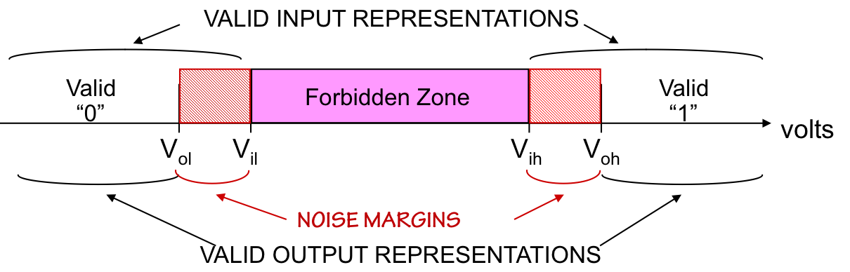
$V_{ol}$:
The highest voltage that represents a valid $0$ at an output
$V_{il}$:
The highest voltage that represents a valid $0$ at an input
$V_{ih}$:
The lowest voltage that represents a valid $1$ at an input
$V_{oh}$:
The lowest voltage that represents a valid $1$ at an output
The impact of the new noise margins on our combinational device abstraction
is that the static discipline now requires each combinational device to
accept marginally valid inputs but produce solidly valid results: the
devices must restore signals that have been degraded by noise
to pristine $0$s and $1$s. This is something that a wire, or any passive
device, cannot do: it requires that the marginal signals be amplified
by increasing their distance from the forbidden zone.
A Combinational Buffer
5.5. A Combinational Buffer
The need for noise margins to maintain signal validity, we have seen, rules out the use of a passive device (like a simple wire) as a combinational device that performs in our digital domain the function of the analog $Copy$ operator described in Section 4.4.
Buffer


Buffer VTC

- That it obeys the functional specification (e.g., any valid 0 input yields a valid 0 output); and
- That it avoids regions that correspond to invalid outputs and valid inputs.

Inverter

Inverter VTC
Gain and nonlinearity requirements
5.6. Gain and nonlinearity requirements
The voltage transfer characteristics for each of these devices -- the buffer and inverter -- are subject to certain geometric constraints imposed by the exclusion of the shaded regions. In each case, the output actually depends upon the input; this implies that the transfer curve must go between valid $0$ and $1$ representations as the input voltage varies. This transition can only be made in the forbidden zone, between the two shaded regions of our voltage input/output plane: any other path would violate the static discipline for some range of input voltages. Note the dimensions of the rectangular gap between the shaded regions: its width is $V_{ih}-V_{il}$, and its height is $V_{oh}-V_{ol}$. The height is necessarily greater than the width, since the height includes our noise margins $V_{il}-V_{ol}$ and $V_{oh}-V_{ih}$ that are excluded by the width. We conclude that the transfer curve must enter this tall, thin rectangle at the top (or bottom) and leave at the bottom (or top) to make the transition between $0$ and $1$. It follows that this region of the curve must be more vertical than horizontal: the magnitude of its average slope as it traverses the forbidden zone must be greater than one. The slope of a voltage transfer curve reflects the gain of the device it describes -- the ratio between an output voltage change and the change in input voltage that caused it. The static discipline and its requirement of non-zero noise margins dictates that combinational devices exhibit gain greater than 1 (or less than -1) in the forbidden zone; this is the mechanism by which they restore marginally valid inputs to produce solid outputs. The gain requirement for combinational devices reinforces our earlier observation that a passive device (such as a wire) does not satisfy the static discipline; some active amplification is required to avoid degeneration of logic values. It is also noteworthy that, since the input and output voltage ranges are identical, the transfer curve must "flatten out" outside of the forbidden zone to compensate for the high gain in that region. Like the example VTCs for the buffer and inverter, the slope (gain) is low for valid $0$ and $1$ inputs, but high between them. The curve must be nonlinear, since its slope necessarily varies over the range of voltages that may be applied. This, along with the requirement for amplification (gain), rules out the use of a simple linear device like a resistor as a combinational device.Constraints on logic mapping parameters
5.7. Constraints on logic mapping parameters
Digital designers don't ordinarily get to choose the logic mapping parameters $V_{ol}$, $V_{il}$, $V_{ih}$, and $V_{oh}$; they are specifications dictated by the family of logic devices being used. Since our goal is a single logic representation scheme to be used by a wide range of devices and operating circumstances, the parameters for a logic family tend to be chosen conservatively. The choice is heavily dependent on the underlying technology being used, as well as other factors such as anticipated range of environmental conditions (temperature, electrical noise, etc) and variability of the manufacturing process. For reliable operation, it is desireable to maximize the noise margins. If we model noise as the injection of a bounded perturbation $V_{noise}$ in connections between devices, we may view noise immunity, defined as the lesser of the two noise margins, as a limit to the magnitude of $V_{noise}$ that our family will tolerate. For this reason, we prefer to equalize the noise margins to the extent possible. The choice of the output parameters $V_{ol}$ and $V_{oh}$ is restricted to the voltages that can be reliably produced by the technology of the logic family. Given values for the output parameters, the choice of valid input ranges dictated by $V_{il}$ and $V_{ih}$ is subject to two opposing goals: (a) the desire to maximize noise margins, and (b) the need for every device in the family to obey the static discipline (i.e., for its transfer curve to avoid forbidden regions).
Ideal inverter VTC
Combinational Timing
5.8. Combinational Timing
Our combinational device abstraction provides a simple guarantee on the timing of output signal validity: whenever all inputs to a combinational device have been stable and valid for the specified propagation delay for that device, each output is guaranteed to be a valid representation of the value dictated by the functional specification for the device. Beyond this promise, there are no validity guarantees on the outputs; in particular, unless all inputs have been valid for at least a propagation delay, an output may be a valid $0$, a valid $1$, or invalid.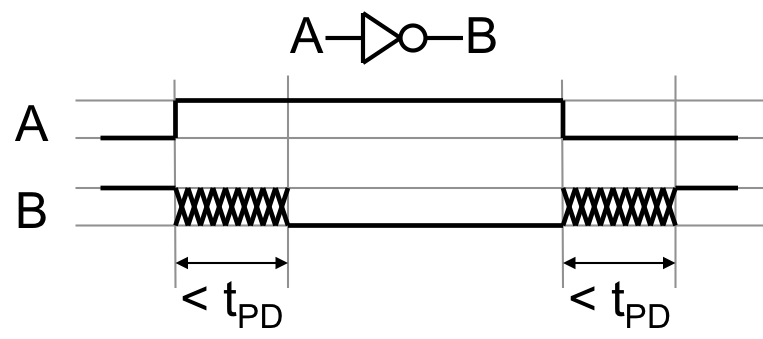
Inverter timing

Cascaded inverters
Optional stronger guarantees
5.9. Optional stronger guarantees
While the combinational device abstraction as described thus far serves the majority of our needs well, there are occasional circumstances where stronger guarantees are necessary. We will encounter an important such case in Chapter 8, when we use combinational devices to build digital memory elements. In this section, we introduce two extensions to the combinational device abstraction to deal with such extenuating circumstances. Each amounts to an additial guarantee that can be specified for a combinational device, extending its timing or functional specification, respectively, beyond our usual standard.Contamination Delay
5.9.1. Contamination Delay
Our combinational device abstraction provides for a propagation delay specification, explicitly recognising the physical reality that it takes some finite time for information in the inputs of a device to propagate to its outputs. The propagation delay is an upper bound on a period of output invalidity; this specification is conservatively chosen, since invalidity of logic signals can cause systems to fail. One can argue for recognition of another, symmetric physical reality: given a device with valid inputs and outputs, it takes finite time for the fact that an input has become invalid to propagate to an output and contaminate its validity. Our model makes the pessimistic assumption that any invalid input immediately contaminates all outputs: all output guarantees are instantly voided by any invalid input. This pessimism is, again, conservative: systems can fail due to invalidity of logic levels, not due to undocumented validity for a brief period after an input change. It is occasionally useful, however, to rely on an output remaining valid for a brief interval after an input becomes invalid. To support these infrequent needs, we introduce a new, optional specification that can augment a combinational device:
contamination delay $t_{CD}$: a specified lower bound on
the time a valid output will persist following an input becoming invalid.
In the usual case, we assume that the contamination delay of a combinational
device is zero -- that is, that an invalid input immediately
contaminates (renders invalid) all outputs. In cases where we require
a nonzero contamination delay, it reflects a minumum time it will take
an invalid input to propagate to (and contaminate) an output.

Inverter Contamination Delay
Lenient combinational devices
5.9.2. Lenient combinational devices
Combinational devices are not required to produce valid outputs unless each of their inputs are valid; using the terminology of denotational semantics, they compute strict functions of their inputs. This characteristic of combinational devices works fine for most of our logic needs, and in the vast majority of cases, all inputs to a combinational device will be valid for a propagation delay before we depend on the validity of its output. However, it is possible (and occasionally useful) to make stronger guarantees, particularly in situations where the output of a function can be deduced when input values have been only partially specified.
Combinational
OR
A lenient combinational device is a
combinational device whose output is guaranteed valid
whenever any combination of inputs sufficient to determine
the output value has been valid for at least $t_{PD}$.
Notice that a lenient combinational device is, in fact, a combinational
device; it is one offering an additional guarantee that it will produce
a valid output when only a subset of its inputs are valid, to the extent
possible.

Lenient OR
Chapter Summary
5.10. Chapter Summary
In this chapter, we have taken a first major step toward the engineering abstraction that underlies digital system engineering: the representation of the discrete variables of our logic model using underlying continuously variable physical parameters. Our representation conventions take care to allow manufacturable devices to conform to realizable specifications made in the logic domain: it is robust in the presence of noise, parasitics, and manufacturing variations that inevitably plague real-world systems. Key elements of this engineering discipline include:- Our 4-parameter mapping convention, using $V_{ol}$, $V_{il}$, $V_{ih}$, and $V_{oh}$ to partition a continuous range of voltages into five distinct regions which define valid representations of logical $1$s and $0$s;
- The separation of valid $0$ and $1$ representations by voltage ranges which do not represent $1$ or $0$;
- The combinational device, an abstract model of logic elements whose specifications include a functional specification (e.g., a truth table) and a propagation delay $t_{pd}$, and which guarantees valid outputs whenever all inputs have been valid for at least $t{pd}$;
- The incorporation of noise margins in our logic mapping, requiring the outputs of combinational devices to adhere to stricter validity standards than the inputs they accept. This important property forces each combinational device to restore marginally valid logic signals to unequivocally valid $1$s and $0$s;
- The fact that acyclic circuits whose components are combinational devices are, themselves, combinational devices. This gives us a simple construction rule for building large systems from a repertoire of small building blocks;
- An optional contamination delay specification, which provides an optional guarantee that outputs of a combinational device remain valid for a short interval after inputs become invalid; and
- The optional stronger guarantee offered by a lenient combinational device, which guarantees valid outputs in cases where functionally irrelevent inputs are invalid.